
Data Sheet


V
DD
p
n
V
DD
V
SS
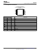
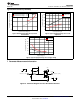
1 (3, 5, 9, 11, 13) A 2 (4, 6, 8, 10, 12)G
G = A
Supply Voltage (V)
Propagation Delay Time (ns)
0 5 10 15 20 25
0
20
40
60
80
100
120
140
D037
CL = 15 pF
CL = 50 pF
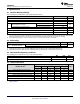
Drain-to-Source Voltage (V)
Output High (Source) Current (mA)
-25 -20 -15 -10 -5 0
-20
-15
-10
-5
0
D004
Gate-to-Source Voltage = -5 V
Gate-to-Source Voltage = -10 V
Gate-to-Source Voltage = -15 V
Load Capacitance (pF)
Propagation Delay Time (ns)
0 20 40 60 80 100 120 140 150
0
20
40
60
80
100
120
D036
VDD = 5 V
VDD = 10 V
VDD = 15 V
9
CD4069UB
www.ti.com
SCHS054E –NOVEMBER 1998–REVISED JANUARY 2019
Product Folder Links: CD4069UB
Submit Documentation FeedbackCopyright © 1998–2019, Texas Instruments Incorporated
Typical Characteristics (continued)
Figure 7. Minimum Output High (Source) Current
Characteristics
Figure 8. Typical Propagation Delay Time vs Load
Capacitance
Figure 9. Typical Propagation Delay Time vs Supply Voltage
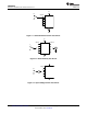
7 Parameter Measurement Information
Figure 10. Schematic Diagram of One of Six Identical Inverters