
Data Sheet


4
CD4069UB
SCHS054E –NOVEMBER 1998–REVISED JANUARY 2019
www.ti.com
Product Folder Links: CD4069UB
Submit Documentation Feedback Copyright © 1998–2019, Texas Instruments Incorporated
(1) Stresses beyond those listed under Absolute Maximum Ratings may cause permanent damage to the device. These are stress ratings
only, which do not imply functional operation of the device at these or any other conditions beyond those indicated under Recommended
Operating Conditions. Exposure to absolute-maximum-rated conditions for extended periods may affect device reliability.
(2) During soldering at distance 1/16 inch ± 1/32 inch (1.59 mm ± 0.79 mm) from case for 10 s maximum
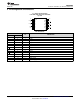
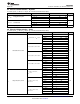
6 Specifications
6.1 Absolute Maximum Ratings
over operating free-air temperature range (unless otherwise noted)
(1)
MIN MAX UNIT
V
DD
DC supply-voltage (voltages referenced to V
SS
terminal) –0.5 20 V
V
I
Input voltage, all inputs –0.5 V
DD
+ 0.5 V
I
IK
DC input current, any one input –10 10 mA
P
D
Power dissipation per package
–55°C to 100°C 500
mW
100°C to 125°C 12 200
Device dissipation per output transistor Full range (all package types) 100 mW
Lead temperature
(2)
265 °C
T
J
Junction temperature 150 °C
T
stg
Storage temperature –65 150 °C
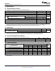
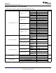
(1) JEDEC document JEP155 states that 500-V HBM allows safe manufacturing with a standard ESD control process.
(2) JEDEC document JEP157 states that 250-V CDM allows safe manufacturing with a standard ESD control process.
6.2 ESD Ratings
VALUE UNIT
V
(ESD)
Electrostatic discharge
Human-body model (HBM), per ANSI/ESDA/JEDEC JS-001
(1)
±500
V
Charged-device model (CDM), per JEDEC specification JESD22-C101
(2)
±200
6.3 Recommended Operating Conditions
over operating free-air temperature range (unless otherwise noted)
MIN MAX UNIT
V
DD
Supply voltage 3 18 V
T
A
Operating temperature –55 125 °C
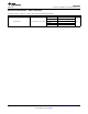
(1) For more information about traditional and new thermal metrics, see the Semiconductor and IC Package Thermal Metrics application
report, SPRA953.
6.4 Thermal Information
THERMAL METRIC
(1)
CD4069UB
UNITD (SOIC) J (CDIP) N (PDIP) NS (SO) PW (TSSOP)
14 PINS 14 PINS 14 PINS 14 PINS 14 PINS
R
θJA
Junction-to-ambient thermal resistance 94.9 — 57.9 91.2 122.1 °C/W
R
θJC(top)
Junction-to-case (top) thermal resistance 56.4 28.5 45.5 48.8 50.8 °C/W
R
θJB
Junction-to-board thermal resistance 49.2 — 37.7 50 63.8 °C/W
ψ
JT
Junction-to-top characterization parameter 21.1 — 30.6 15 6.3 °C/W
ψ
JB
Junction-to-board characterization parameter 48.9 — 37.6 49.6 63.3 °C/W
R
θJC(bot)
Junction-to-case (bottom) thermal resistance N/A N/A N/A N/A N/A °C/W