
Data Sheet
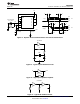
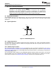
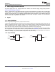


C
V
CC
Logic signal
R
LED
Copyright © 2016,
Texas Instruments Incorporated
14
CD4069UB
SCHS054E –NOVEMBER 1998–REVISED JANUARY 2019
www.ti.com
Product Folder Links: CD4069UB
Submit Documentation Feedback Copyright © 1998–2019, Texas Instruments Incorporated
9 Application and Implementation
NOTE
Information in the following applications sections is not part of the TI component
specification, and TI does not warrant its accuracy or completeness. TI’s customers are
responsible for determining suitability of components for their purposes. Customers should
validate and test their design implementation to confirm system functionality.
9.1 Application Information
The CD4069UB device has a low input current of 1 µA at 18 V over full package-temperature range and 100 nA
at 18 V, 25°C. This device has a wide operating voltage range from 3 V to 18 V and used in high voltage
applications.
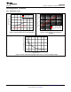
9.2 Typical Application
Figure 20. CD4069UB Application
9.2.1 Design Requirements
The CD4069UB device is the industry's highest logic inverter operating at 18 V under recommended conditions.
The lower drive capabilities makes it suitable for driving light loads like LED and greatly reduces chances of
overshoots and undershoots.
9.2.2 Detailed Design Procedure
The recommended input conditions for Figure 20 includes rise time and fall time specifications (see Δt/ΔV in
Recommended Operating Conditions) and specified high and low levels (see V
IH
and V
IL
in Recommended
Operating Conditions). Inputs are not overvoltage tolerant and must be below V
CC
level because of the presence
of input clamp diodes to V
CC
.
The recommended output condition for the CD4069UB application includes specific load currents. Load currents
must be limited so as to not exceed the total power (continuous current through V
CC
or GND) for the device.
These limits are located in the Absolute Maximum Ratings. Outputs must not be pulled above V
CC
.