
Data Sheet
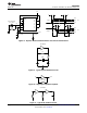
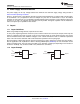


A
1 2
V
DD
= Pin 14
V
SS
= Pin 7
F
G = A
B H = B
C I = C
L = F
E K = E
D J = D
3 4
5 6
9 8
11 10
13 12
13
CD4069UB
www.ti.com
SCHS054E –NOVEMBER 1998–REVISED JANUARY 2019
Product Folder Links: CD4069UB
Submit Documentation FeedbackCopyright © 1998–2019, Texas Instruments Incorporated
8 Detailed Description
8.1 Overview
The CD4069UB device has six inverter circuits. The recommended operating range is from 3 V to
18 V. The CD4069UB-series types are supplied in 14-pin hermetic dual-in-line ceramic packages (F3A suffix),
14-pin dual-in-line plastic packages (E suffix), 14-pin small-outline packages (M, MT, M96, and NSR suffixes),
and 14-pin thin shrink small-outline packages (PW and PWR suffixes).
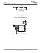
8.2 Functional Block Diagram
8.3 Feature Description
CD4069UB has standardized symmetrical output characteristics and a wide operating voltage range from 3 V to
18 V with quiescent current tested at 20 V. This has a medium operation speed of t
PHL
, t
PLH
= 30 ns (typical) at
10 V. The operating temperature is from –55°C to 125°C. CB4069B meets all requirements of JEDEC tentative
standard No. 13B, Standard Specifications for Description of B Series CMOS Devices.
8.4 Device Functional Modes
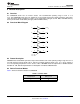
Table 1 shows the functional modes for CD4069UB.
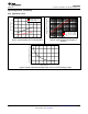
Table 1. Function Table
INPUT
A, B, C, D, E, F
OUTPUT
G, H, I, J, K, L
H L
L H