
Data Sheet
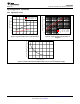


1
2
3
4
5
6
7
14
13
12
11
10
9
8
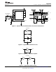
V
DD
500 F
C
L
I
0.1 F
10 kHz
100 kHz, 1 MHz
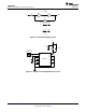
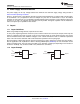
CD4069UB
1/3 CD4069
R
f
OUTIN
S f
DD
P
f
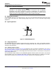
Upper Switching Point :
R R
V
V
R 2
u
f S
DD
N
f
f S
Lower Switching Point :
R R
V
V
R 2
R R
u
!
R
S
12
CD4069UB
SCHS054E –NOVEMBER 1998–REVISED JANUARY 2019
www.ti.com
Product Folder Links: CD4069UB
Submit Documentation Feedback Copyright © 1998–2019, Texas Instruments Incorporated
Figure 18. Input Pulse Shaping Circuit
Figure 19. Dynamic Power Dissipation Test Circuit