
Data Sheet


A
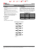
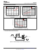
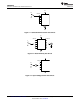
1 2
V
DD
= Pin 14
V
SS
= Pin 7
F
G = A
B H = B
C I = C
L = F
E K = E
D J = D
3 4
5 6
9 8
11 10
13 12
Product
Folder
Order
Now
Technical
Documents
Tools &
Software
Support &
Community
An IMPORTANT NOTICE at the end of this data sheet addresses availability, warranty, changes, use in safety-critical applications,
intellectual property matters and other important disclaimers. PRODUCTION DATA.
CD4069UB
SCHS054E –NOVEMBER 1998–REVISED JANUARY 2019
CD4069UB CMOS hex inverter
1
1 Features
1
• Standardized symmetrical output characteristics
• Medium speed operation: t
PHL
, t
PLH
= 30 ns at 10
V (Typical)
• 100% Tested for quiescent current at 20 V
• Maximum input current of 1 µA at 18 V over full
package-temperature range, 100 nA at 18 V and
25°C
• Meets all requirements of JEDEC tentative
standard No. 13B, Standard Specifications for
Description of B Series CMOS Devices
2 Applications
• Logic inversion
• Pulse shaping
• Oscillators
• High-input-impedance amplifiers
3 Description
The CD4069UB device consist of six CMOS inverter
circuits. These devices are intended for all general-
purpose inverter applications where the medium-
power TTL-drive and logic-level-conversion
capabilities of circuits such as the CD4009 and
CD4049 hex inverter and buffers are not required.
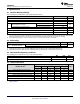
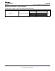
Device Information
(1)
PART NUMBER
PACKAGE
(PINS)
BODY SIZE (NOM)
CD4069UBE PDIP (14) 19.30 mm × 6.35 mm
CD4069UBF CDIP (14) 19.56 mm × 6.67 mm
CD4069UBM SOIC (14) 8.65 mm × 3.91 mm
CD4069UBNSR SO (14) 10.30 mm × 5.30 mm
CD4069UBPW TSSOP (14) 5.00 mm × 4.40 mm
(1) For all available packages, see the orderable addendum at
the end of the data sheet.
CD4069UB Functional Diagram