
Data Sheet


11
10
9
6
A
B
C
INH
134 2 5 1 12 15 14
TG
TG
TG
TG
TG
TG
TG
TG
3
COMMON
OUT/IN
01234567
BINARY
TO
1 OF 8
DECODER
WITH
INHIBIT
LOGIC
LEVEL
CONVERSION
8 7
V
V
SS
EE
16
V
CHANNEL IN/OUT
DD
15
CD4051B
,
CD4052B
,
CD4053B
www.ti.com
SCHS047I –AUGUST 1998–REVISED SEPTEMBER 2017
Product Folder Links: CD4051B CD4052B CD4053B
Submit Documentation FeedbackCopyright © 1998–2017, Texas Instruments Incorporated
8 Detailed Description
8.1 Overview
The CD4051B, CD4052B, and CD4053B analog multiplexers are digitally-controlled analog switches having low
ON impedance and very low OFF leakage current. Control of analog signals up to 20 V
P-P
can be achieved by
digital signal amplitudes of 4.5 V to 20 V (if V
DD
– V
SS
= 3 V, a V
DD
– V
EE
of up to 13 V can be controlled; for
V
DD
– V
EE
level differences above 13 V, a V
DD
– V
SS
of at least 4.5 V is required). For example, if V
DD
= +4.5 V,
V
SS
= 0 V, and V
EE
= –13.5 V, analog signals from –13.5 V to +4.5 V can be controlled by digital inputs of 0 V to
5 V. These multiplexer circuits dissipate extremely low quiescent power over the full V
DD
– V
SS
and V
DD
– V
EE
supply-voltage ranges, independent of the logic state of the control signals. When a logic 1 is present at the
inhibit input terminal, all channels are off.
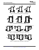
The CD4051B device is a single 8-channel multiplexer having three binary control inputs, A, B, and C, and an
inhibit input. The three binary signals select 1 of 8 channels to be turned on, and connect one of the 8 inputs to
the output.
The CD4052B device is a differential 4-channel multiplexer having two binary control inputs, A and B, and an
inhibit input. The two binary input signals select 1 of 4 pairs of channels to be turned on and connect the analog
inputs to the outputs.
The CD4053B device is a triple 2-channel multiplexer having three separate digital control inputs, A, B, and C,
and an inhibit input. Each control input selects one of a pair of channels which are connected in a single-pole,
double-throw configuration.
When these devices are used as demultiplexers, the CHANNEL IN/OUT terminals are the outputs and the
COMMON OUT/IN terminals are the inputs.
8.2 Functional Block Diagrams
All inputs are protected by standard CMOS protection network.
Figure 26. Functional Block Diagram, CD4051B