
User's Guide


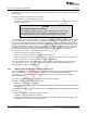
Table Of Contents
- CC3235MODSF SimpleLink™ Wi-Fi® and IoT Solution With MCU LaunchPad™ Hardware
- Table of Contents
- 1 Introduction
- 2 Hardware
- 2.1 Block Diagram
- 2.2 Hardware Features
- 2.2.1 Key Benefits
- 2.2.2 XDS110-Based Onboard Debug Probe
- 2.2.3 Debug Probe Connection: Isolation Jumper Block
- 2.2.4 Application (or "Backchannel") UART
- 2.2.5 JTAG Headers
- 2.2.6 Using the XDS110 Debug Probe with a Different Target
- 2.2.7 Power Connections
- 2.2.8 Reset Pullup Jumper
- 2.2.9 Clocking
- 2.2.10 I2C Connection
- 2.2.11 Sense on Power (SOP)
- 2.2.12 Push-Buttons and LED Indicators
- 2.3 Electrical Characteristics
- 2.4 Antenna Characteristics
- 2.5 BoosterPack™ Plug-in Module Pinout
- 3 Layout Guidelines
- 4 Operational Setup and Testing
- 5 Development Environment Requirements
- 6 Additional Resources
- 7 Assembly Drawing and Schematics
- Appendix A Manual Information to the End User
- Revision History
- Important Notice

TI Confidential – NDA Restrictions
100k
R31
GND
10 ohm
L1
10 ohm
L2
VBUS_USB1
GND
D1+
1
D1-
2
GND
3
D2+
4
D2-
5
NC
6
NC
7
GND
8
NC
9
NC
10
TP
D4S010DQAR
U4
GND
USB-INTERFACE
XDSET_N
XDSET_P
XDSET_ID
VCC_Buffer VCC_LDO_3V3
A
3
VCCA
1
B
4
DIR
5
GND
2
VCCB
6
S
N74LVC1T45DCKR
U3
XDS_nRESET
GND
GNDGND
100k
R28
GND
12
34
56
78
910
J5
61301021121
10k R29
XDS_JTAG_TDI
XDS_JTAG_TDO
XDS_JTAG_TCK
XDS_JTAG_TMS
P19_JTAG_TCK
P20_JTAG_TMS
CC_nRESET
P17_JTAG_TDO
P16_JTAG_TDI
GND
VCC_Buffer
Yellow
D3
XDS_UART_RX
P55_GPIO_01
LP_GPIO_01
VCC_Buffer VCC_LDO_3V3
33.0
R34
A
3
VCCA
1
B
4
DIR
5
GND
2
VCCB
6
SN74LVC1T45DCKR
U5
100k
R33
1
2
3
J11
XDS_UART_TX
P57_GPIO_02
LP_GPIO_02
VCC_Buffer VCC_LDO_3V3
A
3
VCCA
1
B
4
DIR
5
GND
2
VCCB
6
S
N74LVC1T45DCKR
U7
GND
GND
GND
GNDGND
GND
GND
GND
1
2
3
J12
33.0
R
37
GND
to Host-MCUto Targ et
100uF
C27
100uF
C28
270
R35
J9
J10
J7 J8
2.2uH
L3
100k
R36
CHECK LAYOUT GUIDE FROM DATASHEET
POWER MANAGEMENT
TPS62162DSGR
PGND
1
VIN
2
EN
3
AGND
4
FB
5
VOS
6
SW
7
PG
8
EP
9
U6
VBUS_USB1 VCC_MCU_5V
VCC_LDO_3V3 VCC_BRD VCC_Buffer
VBAT_CC
GND
GND GND GND GNDGND GND
VOLTAGE TRANSLATORS
XDS_CC_nRESET
1
2 3
Q1
BSS138
100
R32
VBUS
1
D-
2
D+
3
ID
4
GND
5
6
7
8
11
10
9
J1
1 2
34
SW1
390
R30
10µF
C24
10µF
C26
22µF
C25
Red
D4
0.1uF
C19
0.1uF
C20
0.1uF
C22
0.1uF
C23
0.1uF
C2
9
0.1uF
C3
0
0.01µF
C21
www.ti.com
Assembly Drawing and Schematics
45
SWRU548A–February 2019–Revised August 2019
Submit Documentation Feedback
Copyright © 2019, Texas Instruments Incorporated
CC3235MODSF LaunchPad™ Development Kit (LAUNCHCC3235MOD)
Figure 33. Schematics (2 of 5)