
User's Guide
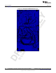
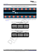
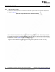
Table Of Contents
- CC3235MODSF SimpleLink™ Wi-Fi® and IoT Solution With MCU LaunchPad™ Hardware
- Table of Contents
- 1 Introduction
- 2 Hardware
- 2.1 Block Diagram
- 2.2 Hardware Features
- 2.2.1 Key Benefits
- 2.2.2 XDS110-Based Onboard Debug Probe
- 2.2.3 Debug Probe Connection: Isolation Jumper Block
- 2.2.4 Application (or "Backchannel") UART
- 2.2.5 JTAG Headers
- 2.2.6 Using the XDS110 Debug Probe with a Different Target
- 2.2.7 Power Connections
- 2.2.8 Reset Pullup Jumper
- 2.2.9 Clocking
- 2.2.10 I2C Connection
- 2.2.11 Sense on Power (SOP)
- 2.2.12 Push-Buttons and LED Indicators
- 2.3 Electrical Characteristics
- 2.4 Antenna Characteristics
- 2.5 BoosterPack™ Plug-in Module Pinout
- 3 Layout Guidelines
- 4 Operational Setup and Testing
- 5 Development Environment Requirements
- 6 Additional Resources
- 7 Assembly Drawing and Schematics
- Appendix A Manual Information to the End User
- Revision History
- Important Notice

TI Confidential – NDA Restrictions
S
W
Layout Guidelines
www.ti.com
36
SWRU548A–February 2019–Revised August 2019
Submit Documentation Feedback
Copyright © 2019, Texas Instruments Incorporated
CC3235MODSF LaunchPad™ Development Kit (LAUNCHCC3235MOD)
Figure 24 shows the top view of the coplanar waveguide with GND and via stitching.
Figure 24. CPW With GND and Via Stitching (Top View)
The recommended values for the PCB are provided for 2-layer boards in Table 10 and for 4-layer boards
in Table 11.
Table 10. Recommended PCB Values for 2-Layer Board
(L1 to L2 = 42.1 mils)
PARAMETER VALUE UNIT
W 26 mils
S 5.5 mils
H 42.1 mils
Er (FR-4 substrate) 4.2 F/m
Table 11. Recommended PCB Values for 4-Layer Board
(L1 to L2 = 16 mils)
PARAMETER VALUE UNITS
W 21 mils
S 10 mils
H 16 mils
Er (FR-4 substrate) 4.5 F/m