
User's Guide


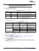
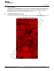

Table Of Contents
- CC3235MODSF SimpleLink™ Wi-Fi® and IoT Solution With MCU LaunchPad™ Hardware
- Table of Contents
- 1 Introduction
- 2 Hardware
- 2.1 Block Diagram
- 2.2 Hardware Features
- 2.2.1 Key Benefits
- 2.2.2 XDS110-Based Onboard Debug Probe
- 2.2.3 Debug Probe Connection: Isolation Jumper Block
- 2.2.4 Application (or "Backchannel") UART
- 2.2.5 JTAG Headers
- 2.2.6 Using the XDS110 Debug Probe with a Different Target
- 2.2.7 Power Connections
- 2.2.8 Reset Pullup Jumper
- 2.2.9 Clocking
- 2.2.10 I2C Connection
- 2.2.11 Sense on Power (SOP)
- 2.2.12 Push-Buttons and LED Indicators
- 2.3 Electrical Characteristics
- 2.4 Antenna Characteristics
- 2.5 BoosterPack™ Plug-in Module Pinout
- 3 Layout Guidelines
- 4 Operational Setup and Testing
- 5 Development Environment Requirements
- 6 Additional Resources
- 7 Assembly Drawing and Schematics
- Appendix A Manual Information to the End User
- Revision History
- Important Notice

TI Confidential – NDA Restrictions
www.ti.com
Layout Guidelines
29
SWRU548A–February 2019–Revised August 2019
Submit Documentation Feedback
Copyright © 2019, Texas Instruments Incorporated
CC3235MODSF LaunchPad™ Development Kit (LAUNCHCC3235MOD)
3 Layout Guidelines
The integrator of the CC3235MODx !~and CC3235MODAx modules must comply with the PCB layout
recommendations described in the following subsections to preserve and minimize the risk with regulatory
certifications for FCC, ISED/IC, ETSI/CE, and MIC. Also, TI recommends that customers follow the
guidelines described in this section to achieve similar performance.
3.1 LAUNCHCC3235MOD Board Layout
The reference layout consists of a four-layer design. Figure 17 shows the LAUNCHCC3235MOD top layer.
Figure 17. LAUNCHCC3235MOD Top Layer