
User's Guide
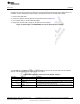
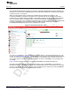
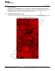

Table Of Contents
- CC3235MODSF SimpleLink™ Wi-Fi® and IoT Solution With MCU LaunchPad™ Hardware
- Table of Contents
- 1 Introduction
- 2 Hardware
- 2.1 Block Diagram
- 2.2 Hardware Features
- 2.2.1 Key Benefits
- 2.2.2 XDS110-Based Onboard Debug Probe
- 2.2.3 Debug Probe Connection: Isolation Jumper Block
- 2.2.4 Application (or "Backchannel") UART
- 2.2.5 JTAG Headers
- 2.2.6 Using the XDS110 Debug Probe with a Different Target
- 2.2.7 Power Connections
- 2.2.8 Reset Pullup Jumper
- 2.2.9 Clocking
- 2.2.10 I2C Connection
- 2.2.11 Sense on Power (SOP)
- 2.2.12 Push-Buttons and LED Indicators
- 2.3 Electrical Characteristics
- 2.4 Antenna Characteristics
- 2.5 BoosterPack™ Plug-in Module Pinout
- 3 Layout Guidelines
- 4 Operational Setup and Testing
- 5 Development Environment Requirements
- 6 Additional Resources
- 7 Assembly Drawing and Schematics
- Appendix A Manual Information to the End User
- Revision History
- Important Notice

TI Confidential – NDA Restrictions
Hardware
www.ti.com
28
SWRU548A–February 2019–Revised August 2019
Submit Documentation Feedback
Copyright © 2019, Texas Instruments Incorporated
CC3235MODSF LaunchPad™ Development Kit (LAUNCHCC3235MOD)
Figure 16. LAUNCHCC3235MOD BoosterPack™ Header Pin Assignments
NOTE: RESET output is an open-drain-type output and can only drive the pin low. The pullup
ensures that the line is pulled back high when the button is released. No external
BoosterPack can drive this pin low.
All the signals are referred to by the pin number in the SDK; Figure 16 shows the default mappings. Some
of the pins are repeated across the connector. For instance, pin 62 is available on P1 and P4, but only P1
is connected by default. The signal on P4 is marked with an asterisk (*) to signify that it is not connected
by default. The signal can be routed to the pin by using a 0-Ω resistor in the path. For the exact resistor
placement, see the CC3235MODSF SimpleLink
TM
Wi-Fi
®
Wireless MCU LaunchPad Board Design Files.