
User's Manual
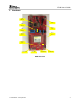
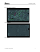
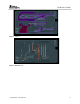
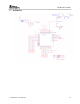
Table Of Contents

EVM User’s Guide
TI Confidential – Strictly Private 7
CC3200
P1 P3
Ref
Signal
Dev
Pin#
Dev
Pin#
Signal
1
3.3V
5V
2
ADC_CH1
58
GND
3
UART0_RX
4 57
ADC_CH0
4
UART0_TX
3 60
ADC_CH3
5
GPIO
61
58*
ADC_CH1
6
ADC_CH2
59
59*
ADC_CH2
7
SPI_CLK
5 63
AUD_SYNC
8
GPIO
62 53
AUD_CLK
9
I2C_SCL
1 64
AUD_DOUT
10
I2C_SDA
2 50
AUD_DIN
P4 P2
Signal
Dev
Pin#
Dev
Pin#
Signal
Ref
PWM
2*
GND
1
PWM
1*
18
GPIO
2
PWM
17*
8
SPI_CS
3
PWM
64*
45
GPIO
4
CCAP/GPIO
21*
RESET_OUT
5
CCAP/GPIO
18*
7
SPI_DOUT
6
GPIO
62*
6
SPI_DIN
7
GPIO
60*
21
GPIO
8
GPIO
16
55
GPIO
9
GPIO
17
15
GPIO
10
The signal mappings are as per the table above. All the signals are referred by the pin-no in the
SDK and the table above shows the default mappings. Note that some of the pins are repeated
across the connector. For e.g. pin 62 is available on P1 and P4, but only P1 is connected by
default. The signal on P4 is marked with a *(star) to signify that is not connected by default. It
can be routed to the pin by using a 0 Ohm resistor in the path. Please refer to the schematics
and placement diagram for the exact resistor placement.
2.3 Power
The Launchpad is designed to work from the USB provided power supply as it
enumerates as a bus-powered device. Care has been taken in the design to ensure that
the board does not violate the in-rush limits of the USB bus. The board can also be
powered by an external 2xAA or 2xAAA battery which is connected on J20.