
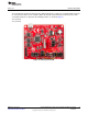
User manual

CC3200
P1 P3
Ref Signal
Dev
Pin#
Dev
Pin# Signal
1 3.3V 5V
2 ADC_CH1 58 GND
3 UART0_RX 4 57 ADC_CH0
4 UART0_TX 3 60 ADC_CH3
5 GPIO 61 58* ADC_CH1
6 ADC_CH2 59 59* ADC_CH2
7 SPI_CLK 5 63 AUD_SYNC
8 GPIO 62 53 AUD_CLK
9 I2C_SCL 1 64 AUD_DOUT
10 I2C_SDA 2 50 AUD_DIN
P4 P2
Signal
Dev
Pin#
Dev
Pin# Signal Ref
PWM 2* GND 1
PWM 1* 18 GPIO 2
PWM 17* 8 SPI_CS 3
PWM 64* 45 GPIO 4
CCAP/GPIO 21*
RESET_OUT 5
CCAP/GPIO 18* 7 SPI_DOUT 6
GPIO 62* 6 SPI_DIN 7
GPIO 60* 21 GPIO 8
GPIO 16 55 GPIO 9
GPIO 17 15 GPIO 10
Hardware Description
www.ti.com
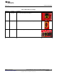
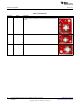
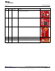
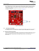
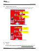
2.4.8 2x20 Pin Connector Assignment
The signal assignment on the 2x20 pin connector is shown in Figure 8. The P1-Pn naming convention is
used for 2x20 pin connectors only.
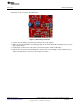
Figure 8. 2x20 Pin Connector
The signal mappings are as indicated in above table shown in Figure 8. All the signals are referred by the
pin number in the SDK and Figure 8 shows the default mappings. Note that some of the pins are repeated
across the connector. For instance, pin 62 is available on P1 and P4, but only P1 is connected by default.
The signal on P4 is marked with a *(star) to signify that it is not connected by default. It can be routed to
the pin by using a 0 Ω resistor in the path. For the exact resistor placement, see the schematics and
placement diagram.
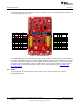
2.5 Power
The LaunchPad is designed such that it can be powered by the USB connection or by external
2xAA/2xAAA batteries.
14
CC3200 SimpleLink™ Wi-Fi
®
and IoT Solution with MCU LaunchPad SWRU372–June 2014
Hardware
Submit Documentation Feedback
Copyright © 2014, Texas Instruments Incorporated