
User's Manual
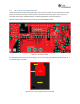

6.4 AntennaPlacementandRouting
TheantennaistheelementusedtoconverttheguidedwavesonthePCBtracestothefreespace
electromagneticradiation.Theplacementandlayoutoftheantennaarethekeystoincreasedrangeand
datarates.Table6‐2providesa summaryoftheantennaguidelines.
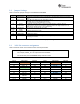
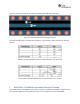
Item Guidelines
1 PlacetheantennaonanedgeorcornerofthePCB.
2 EnsurethatnosignalsareroutedacrosstheantennaelementsonallthelayersofthePCB.
3 Mostantennas,includingthechipantennausedontheboosterpack,requireground
clearanceonallthelayersofthePCB.Ensurethatthegroundisclearedoninnerlayersas
well.
4 Ensurethatthereisprovisiontoplacematchingcomponentsfortheantenna.Thesemustbe
tunedforbestreturnlosswhenthecompleteboardisassembled.Any plasticsorcasingmust
alsobemountedwhiletuningtheantennabecausethiscanimpacttheimpedance.
5 Ensurethattheantennaimpedance is50Ωbecausethedeviceisratedtowork onlywitha
50‐Ωsystem.
6 Incaseofprintedantenna,ensurethatthesimulationisperformedwiththesoldermaskin
consideration.
7 Ensurethattheantennahasanearomni‐directionalpattern.
8 Thefeedpointoftheantennaisrequiredtobegrounded.Thisis onlyfortheantennatype
usedontheCC3120MODBoosterPack.Refertothespecificantennadatasheetsforthe
recommendations.
Table6‐2:AntennaGuidelines
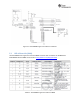
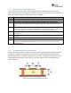
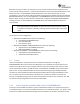
6.5 TransmissionLineConsiderations
TheRFsignalfromthedeviceisrouted tothe antennausingaCoplanarWaveguidewithground(CPW‐
G)structure.TheCPW‐Gstructureoffersthemaximumamountofisolationandthebestpossible
shieldingtotheRFlines.InadditiontothegroundontheL1 layer,placingGNDvias
alongthelinealso
providesadditionalshielding.Figure6‐5showsacrosssectionofthecoplanarwaveguidewiththe
criticaldimensions.
Figure6‐5:CoplanarWaveguide(Cros sSection)