
User's Manual
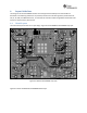

2.2 JumperSettings
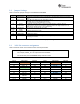
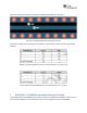
Table2‐3liststhe jumpersettingsontheBOOSTXL‐CC3120MD
Reference
Usage
Comments
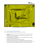
J7
USB connector
For powering the BoosterPack when connected with a LaunchPad which cannot source enough
current.
di
(f
l
J8
Power selection
Choose the power supply from the LauchPad kit or the on-
board USB. J8 (1-2) power from MCU LaunchPad
J8 (2-3) power from on-board USB using 3.3 V LDO
J6
Current
measurement
For Hibernate and LPDS currents, connect an ammeter across J6 : Range (< 500 µA)
For Active current, mount a 0.1 Ω resistor on R35 and measure the voltage across the 0.1 Ω
resistor using a voltmeter (range (< 50 mV peak-peak)).
P1, P2,
P3, P4
BoosterPack
header
2x10 pins each connected to the LaunchPad.
J3 LED EN. For Enabling/Disabling the LED’s.
J4
Reset Pullup For keeping the reset up
J2
RF Test U.FL connector for conducted testing in the lab. Using this requires an ECO to be made to the board
by swapping two resistors.
Table2‐3:BOOSTXL‐CC3120MODjumpersettings
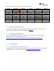
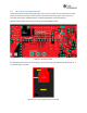
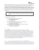
2.3 2x20Pinconnectorassignment
Table2‐4liststhe outerrowconnectorsofthetwo20‐pinheaders.
Note: Allsignalsare3.3VCMOSlogiclevelsandarereferredwithrespecttotheCC3120IC.
Forexample,UART1_TXisanoutputfromtheCC3120IC.
FortheSPIlines,theCC3120MODalwaysactslike
aslave
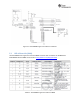
Pin
No
Signal Name
Direction Pin
No
Signal Name
Direction
P1.1
VCC (3.3 V)
IN P2.1 GND
IN
P1.2
UNUSED
NA P2.2 IRQ
OUT
P1.3
UART1_TX
OUT P2.3
SPI_CS
IN
P1.4
UART1_RX
IN P2.4
UNUSED
NA
P1.5
nHIB
IN P2.5
nRESET
IN
P1.6
UNUSED
NA P2.6
SPI_MOSI
IN
P1.7
SPI_CLK
IN P2.7
SPI_MISO
OUT
P1.8
FACTORY
DEFAULT
NA P2.8
UNUSED
NA
P1.9
UNUSED
NA P2.9
UNUSED
NA
P1.10
UNUSED
NA P2.10
UNUSED
NA
Table2‐4:BOOSTXL‐CC3120MODouterrowpinconnectors