
User's Manual


CC3100BOOST User Guide
TI Proprietary Information - Strictly Private
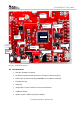
4 Layer PCB with 6mil spacing and track width.
3.3 Jumper and connector information
3.3.1
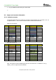
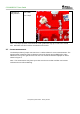
2x20 pin connector
The signal assignment on the 2x20 pin connector is shown below. The convention of J1..J4
is replaced with P1…P4 to avoid confusion with the actual board reference.
Outer row connectors
Pin No
Signal Name
Direction
Pin No
Signal Name
Direction
P1.1
VCC(3.3V)
IN
P2.1
GND
IN
P1.2
UN-USED
NA
P2.2
IRQ
OUT
P1.3
UART1_TX
OUT
P2.3
SPI_CS
IN
P1.4
UART1_RX
IN
P2.4
UN-USED
NA
P1.5
nHIB
IN
P2.5
nRESET
IN
P1.6
UNUSED
NA
P2.6
SPI_MOSI
IN
P1.7
SPI_CLK
IN
P2.7
SPI_MISO
OUT
P1.8
UN-USED
NA
P2.8
UN-USED
NA
P1.9
UN-USED
NA
P2.9
UN-USED
NA
P1.10
UN-USED
NA
P2.10
UN-USED
NA
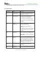
Inner row connectors
Pin No
Signal Name
Direction
Pin No
Signal Name
Direction
P3.1
+5V
IN
P4.1
ANT_SEL_1
OUT
P3.2
GND
IN
P4.2
ANT_SEL_2
OUT
P3.3
UN-USED
NA
P4.3
UN-USED
NA
P3.4
UN-USED
NA
P4.4
UART1_CTS
IN
P3.5
UN-USED
NA
P4.5
UART1_RTS
OUT
P3.6
UN-USED
NA
P4.6
UN-USED
NA
P3.7
UN-USED
NA
P4.7
NWP_LOG_TX
OUT
P3.8
UN-USED
NA
P4.8
WLAN_LOG_TX
OUT
P3.9
UN-USED
NA
P4.9
WL_RS232_RX
IN
P3.10
UN-USED
NA
P4.10
WL_RS232_TX
OUT
Note : All signals are 3.3V COMS logic levels and is referred w.r.t. CC3100 IC. For e.g.
UART1_TX is an output from the CC3100.