
User's Manual
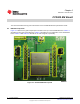
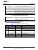

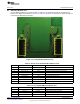
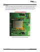
Table Of Contents

EM Board Top View
www.ti.com
Table 2-4. Header J5 of the CC3000 EM Board Top View
J5 Pin Pin Name Pin Type Descriptions
1 SCL_CC3000
(1)
Output I2C clock signal output from the CC3000 module. This
pin is connected to SCL_EEPROM through a 0-Ω
resistor and is not used by end users.
2 SCL_EEPROM
(1)
Input I2C clock signal input from EEPROM inside the CC3000
module. This pin is connected to SCL_CC3000 using a
0-Ω resistor and is not used by end users.
3 SDA_CC3000
(1)
Input/Output I2C data signal from the CC3000 module. This pin is
connected to SDA_EEPROM using a 0-Ω resister and is
not used by end users.
4 SDA_EEPROM
(1)
Input/Output I2C data signal from EEPROM inside the CC3000
module. This pin is connected to the SDA_CC3000
device using a 0-Ω resistor and is not used by end users.
5 VBAT_SW_EN Input Active-high enables the signal from the host device.
6 GND – Ground
7 GND – Ground
8 VIO_HOST Power In VIO power supply from the host to the module. For the
MSP430 host platform, VIO_HOST = VBAT_IN. For other
platforms that have different voltage levels from battery
voltages, R14 can be removed.
9 VBAT_IN Power In Battery voltage input to module. For the MSP430 host
platform, VIO_HOST = VBAT_IN. For other platforms
that have different voltage levels from the battery
voltages, R14 can be removed.
10 GND – Ground
11 Reserved – Reserved
(1)
The EM board arrives with EEPROM preprogrammed.
8
CC3000 EM Board SWRU326–November 2012
Submit Documentation Feedback
Copyright © 2012, Texas Instruments Incorporated