
User's Manual
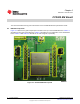

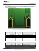
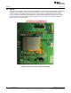
Table Of Contents

www.ti.com
List of Figures
2-1. CC3000 EM Board Top View.............................................................................................. 6
2-2. CC3000 EM Board Bottom View.......................................................................................... 9
2-3. Antenna Location and RF Trace Routing .............................................................................. 10
2-4. Matching Circuit Between the Antenna and the CC3000 EM Board ............................................... 11
2-5. Return Loss from the ACX Antenna and Matching Circuit........................................................... 11
2-6. Antenna Radiation Patterns.............................................................................................. 12
2-7. Host PCB Mating Connector Arrangement ............................................................................ 13
2-8. Schematics of the CC3000 EM Board.................................................................................. 14
3-1. Module Layout Guidelines................................................................................................ 16
3-2. Module Layout Guidelines................................................................................................ 17
3-3. Trace Design for the PCB Layout ....................................................................................... 18
3-4. Layer 1 Combined With Layer 2......................................................................................... 18
3-5. Antenna and RF Trace Routing Layout Guidelines................................................................... 19
3-6. Power Supply Routing of the CC3000 EM Board ..................................................................... 20
4-1. MSP-EXP430FR5739 Test Platform and CC3000 EM Board....................................................... 21
List of Tables
2-1. Key Parts of CC3000 EM Board Top View .............................................................................. 7
2-2. J2 Configuration of the CC3000 EM Board.............................................................................. 7
2-3. Header J4 of the CC3000 EM Board Top View......................................................................... 7
2-4. Header J5 of the CC3000 EM Board Top View......................................................................... 8
2-5. Header J6 of CC3000 EM Board Bottom View ......................................................................... 9
2-6. J7 of CC3000 EM Board Bottom View ................................................................................... 9
2-7. BOM for the TI CC3000 EM Board...................................................................................... 15
3-1. Module Layout Guidelines................................................................................................ 17
3-2. Trace Design Measurement Values .................................................................................... 18
3-3. Antenna and RF Trace Routing Layout Guidelines................................................................... 19
3
SWRU326–November 2012 List of Figures
Submit Documentation Feedback
Copyright © 2012, Texas Instruments Incorporated