
User's Manual
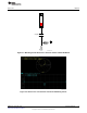
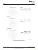

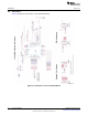
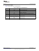
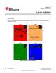


Table Of Contents

SWRU326-015
SWRU326-010
www.ti.com
Figure 3-3. Trace Design for the PCB Layout
Figure 3-4. Layer 1 Combined With Layer 2
Table 3-2. Trace Design Measurement Values
Measurement Length
H (height between L1 and L2) 12.0 mil
W (RF trace) 14.3 mil
T (thickness) 1.2 mil
S (separation) 10.0 mil
ε
r
(dielectric) 4.3
18
Layout Guidelines SWRU326–November 2012
Submit Documentation Feedback
Copyright © 2012, Texas Instruments Incorporated