TI CC3000 Evaluation Module User's Guide Literature Number: SWRU326 November 2012
Contents 4 ....................................................................................................................................... 4 Introduction ........................................................................................................................ 5 CC3000 EM Board ............................................................................................................... 6 2.1 EM Board Top View .........................................................................
www.ti.com List of Figures 2-1. CC3000 EM Board Top View.............................................................................................. 6 2-2. CC3000 EM Board Bottom View .......................................................................................... 9 2-3. Antenna Location and RF Trace Routing 10 2-4. Matching Circuit Between the Antenna and the CC3000 EM Board 11 2-5. 2-6. 2-7. 2-8. 3-1. 3-2. 3-3. 3-4. 3-5. 3-6. 4-1. ...................................................
Preface SWRU326 – November 2012 Read This First About This Manual This user guide describes how to use the TI CC3000 evaluation module (EM) board to evaluate the performance of the TI CC3000 module. Related Documentation From Texas Instruments • • TI SimpleLink™ CC3000 Module – Wi-Fi 802.11b/g Network Processor Data Sheet (SWRS126) CC3000 Wiki for MCU: http://processors.wiki.ti.com/index.
Chapter 1 SWRU326 – November 2012 Introduction This user guide describes how to use the TI CC3000 evaluation module (EM) board to evaluate the performance and functionality of the TI CC3000 module. The CC3000 module is a self-contained Wi-Fi® solution that enables internet connectivity for a wide variety of microcontroller (MCU) systems. The SimpleLink Wi-Fi from TI minimizes the host MCU software requirements, making it ideal for low-power and low-cost applications.
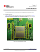
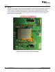
Chapter 2 SWRU326 – November 2012 CC3000 EM Board This section describes the key parts and features of the CC3000 EM board top and bottom views. 2.1 EM Board Top View Figure 2-1 shows the key parts and jumpers mounted on the top of the CC3000 EM board. Table 2-1 describes the key parts of the EM board. Table 2-2 describes the J2 configuration of the CC3000 EM board. Table 2-3 and Table 2-4 describe the J4 and J5 signals, respectively. Figure 2-1.
EM Board Top View www.ti.com Table 2-1. Key Parts of CC3000 EM Board Top View Key Parts Descriptions CC3000MOD Core module for performance evaluation (for more information, see the CC3000 module data sheet). Antenna Can be used for radiated testing by reworking the capacitor to correct pads J1 U.FL RF connector used for conductive RF test J2 Used to switch between test mode and operation mode. When pins 2 and 3 are shorted, J2 runs in operation mode.
EM Board Top View www.ti.com Table 2-4. Header J5 of the CC3000 EM Board Top View J5 Pin 1 (1) 8 Pin Name SCL_CC3000 Pin Type (1) Output Descriptions I2C clock signal output from the CC3000 module. This pin is connected to SCL_EEPROM through a 0-Ω resistor and is not used by end users. 2 SCL_EEPROM (1) Input I2C clock signal input from EEPROM inside the CC3000 module. This pin is connected to SCL_CC3000 using a 0-Ω resistor and is not used by end users.
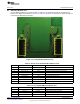
EM Board Bottom View www.ti.com 2.2 EM Board Bottom View The two EM board mating connectors J6 and J7 connect to the host platform and are mounted on the bottom of the EM board, as shown in Figure 2-2. Table 2-5 and Table 2-6 describe the signals brought out from these two EM mating connectors. SWRU326-002 Figure 2-2. CC3000 EM Board Bottom View Table 2-5.
Antenna 2.3 www.ti.com Antenna The ACX ceramic antenna is mounted on the EM board with a specific layout and matching circuit for the radiation tests conducted in FCC, CE, and IC certifications. Figure 2-3 shows the location of the ACX ceramic antenna on the EM board and the RF trace routing from the CC3000 module to the antenna. Figure 2-4 shows the matching circuit between the antenna and the EM board. The return loss is based on the matching circuit and RF trace routing, as shown in Figure 2-5.
Antenna www.ti.com AT8010-E2R9HAA 2.2 pF 2.2 nH SWRU326-004 Figure 2-4. Matching Circuit Between the Antenna and the CC3000 EM Board SWRU326-005 Figure 2-5.
Antenna www.ti.com XY plane Unit : dBi Peak gain Avg. gain 0.3 –2.6 XY plane XZ plane Peak gain Avg. gain 1.3 –4.2 Peak gain Avg. gain 0.9 –0.9 XZ plane YZ plane YZ plane SWRU326-006 Figure 2-6.
Hardware Setup www.ti.com 2.4 Hardware Setup Before conducting performance tests, the EM board must be connected to the host platform, either with the mating connectors (J6 and J7) or the single-row headers (J4 and J5). To use the EM mating connectors to connect the hardware, the mating EM connector must be lined up and spaced 1.2 inches apart (see Figure 2-7). To use the single-row headers, the required signals from the EM mating connectors must be wired to the host platform. 1.
Schematics 2.5 www.ti.com Schematics Figure 2-8 shows the schematics of the CC3000 EM board. SWRU326-008 Figure 2-8.
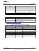
Bill of Materials (BOM) www.ti.com 2.6 Bill of Materials (BOM) Table 2-7 lists the BOM for the TI CC3000 EM board. Table 2-7. BOM for the TI CC3000 EM Board Items Reference Designator 1 U1 2 ANT1 3 J1 Mini RF header receptacle 4 J2 CON male 1 x 3, pitch 2.0 mm 5 J3 CON male 1 x 2, pitch 2.0 mm 6 J6,J7 Female header, Fool Proof H:4.3, 2 x 10, pitch 1.27 mm, SMT 7 C1,C3 CAP 0402 10 pF, 50 V, NPO, ±5% 8 C4,C5 CAP 0402 1 µF, X5R, 6.
Chapter 3 SWRU326 – November 2012 Layout Guidelines This section presents guidelines that must be followed when creating a board design incorporating the TI CC3000 module. Figure 3-1 shows the TI CC3000 EM four-layer board. Table 3-1 and Figure 3-2 describe instances of good layout practices. SWRU326-014 Figure 3-1.
www.ti.com Table 3-1. Module Layout Guidelines Reference (1) (1) Guideline Description 1 The proximity of ground vias must be close to the pad. 2 Signal traces must not be run underneath the module on the layer where the module is mounted. 3 Have a complete ground pour in layer 2 for thermal dissipation. 4 Have a solid ground plane and ground vias under the module for stable system and thermal dissipation.
www.ti.com SWRU326-010 Figure 3-3. Trace Design for the PCB Layout SWRU326-015 Figure 3-4. Layer 1 Combined With Layer 2 Table 3-2. Trace Design Measurement Values 18 Measurement Length H (height between L1 and L2) 12.0 mil W (RF trace) 14.3 mil T (thickness) 1.2 mil S (separation) 10.0 mil εr (dielectric) 4.
www.ti.com Table 3-3. Antenna and RF Trace Routing Layout Guidelines Reference (1) (1) Guideline Description 1 The RF trace antenna feed must be as short as possible beyond the ground reference. At this point, the trace starts to radiate. 2 The RF trace bends must be gradual with an approximate maximum bend of 45 degrees with trace mitered. RF traces must not have sharp corners. 3 RF traces must have via stitching on the ground plane beside the RF trace on both sides.
www.ti.com Figure 3-6 shows the supply routing guidelines: • For power supply routing, the power trace for VBAT must be at least 40 mil wide. • The 1.8-V trace must be at least 18 mil wide. • Make VBAT traces as wide as possible to ensure reduced inductance and trace resistance. • If possible, shield VBAT traces with ground above, below, and beside the traces. SWRU326-012 Figure 3-6.
Chapter 4 SWRU326 – November 2012 Application Development TI • • • • • • supports the CC3000 EM board when paired with the following TI MCU host platforms: MSP-EXP430FR5739 MSP-EXP430F5529 MSP-EXP430F5438 MSP-EXP430FG4618 DK-LM3S9B96 EK-LM4F232 To find example applications for each of the listed host platforms, go to the TI wiki at: http://processors.wiki.ti.com/index.php/CC3000_Wi-Fi_for_MCU#TI_Platforms.
IMPORTANT NOTICE Texas Instruments Incorporated and its subsidiaries (TI) reserve the right to make corrections, enhancements, improvements and other changes to its semiconductor products and services per JESD46, latest issue, and to discontinue any product or service per JESD48, latest issue. Buyers should obtain the latest relevant information before placing orders and should verify that such information is current and complete.
REGULATORY COMPLIANCE INFORMATION When the radio module is included in a final product, the following warning statements must be included in the final product user guide Caution This device complies with part 15 of the FCC Rules. Operation is subject to the following two conditions: (1) This device may not cause harmful interference, and (2) this device must accept any interference received, including interference that may cause undesired operation.