
User manual


www.ti.com
Peripheral PORTIDs
11.9 Peripheral PORTIDs
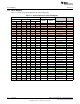
Table 11-3 lists the different PORTID signals.
Table 11-3. CC26xx Chameleon Family PORTIDs
ID PortName Port Description ID PortName Port Description
0 GPIO Default GPIO usage 27 MCU_GPTM_GPTM4 GMTM timer pin GPTM4
1 AON_SCS AON SPI-S SCS pin 28 MCU_GPTM_GPTM5 GMTM timer pin GPTM5
2 AON_SCK AON SPI-S SCK pin 29 MCU_GPTM_GPTM6 GMTM timer pin GPTM6
3 AON_SDI AON SPI-S SDI pin 30 MCU_GPTM_GPTM7 GMTM timer pin GPTM7
4 AON_SDO AON SPI-S SDO pin 31 Reserved
5-6 Reserved 32 MCU_CM3_SWV CM3 SWV
7 AON_CLK32K AON 32-kHz clock pin 33 MCU_SSI1_RX SSI 1 Rx pin
8 AUX_IO AUX I/O pin 34 MCU_SSI1_TX SSI 1 Tx pin
9 MCU_SSI0_RX SSI 0 Rx pin 35 MCU_SSI1_FSS SSI 1 FSS pin
10 MCU_SSI0_TX SSI 0 Tx pin 36 MCU_SSI1_CLK SSI 1 CLK pin
11 MCU_SSI0_FSS SSI 0 FSS pin 37 MCU_I2S_AD0 I2S Data 0 pin
12 MCU_SSI0_CLK SSI 0 CLK pin 38 MCU_I2S_AD1 I2S Data 1 pin
13 MCU_I2C_MSSDA I2C Data 39 MCU_I2S_WCLK I2S WCLK pin
14 MCU_I2C_MSSCL I2C Clock 40 MCU_I2S_BCLK I2S BCLK pin
15 MCU_UART0_RX UART 0 Rx pin 41 MCU_I2S_MCLK I2S MCLK pin
16 MCU_UART0_TX UART 0 Tx pin 42- Reserved
45
17 MCU_UART0_CTS UART 0 CTS pin 46 RF Core internal signal
18 MCU_UART0_RTS UART 0 RTS pin 47 RFC_GPO0
19- Reserved 48 RFC_GPO1
22
23 MCU_GPTM_GPTM0 GMTM timer pin GPTM0 49 RFC_GPO2
24 MCU_GPTM_GPTM1 GMTM timer pin GPTM2 50 RFC_GPO3
25 MCU_GPTM_GPTM2 GMTM timer pin GPTM3 51- RF Core internal signals
56
26 MCU_GPTM_GPTM3 GMTM timer pin GPTM4
11.10 I/O Pin
This section discusses specific physical details and configuration possibilities for the I/O pins on the
CC26xx devices.
11.10.1 Physical Pin
The digital I/O driver and receiver is a wide-supply voltage range, bidirectional buffer combining an output
buffer, an input buffer with optional hysteresis, and optional pullup and pulldown circuitry. The I/O has
limited power-management features, including support for wakeup from sleep with core power gated. The
sink and source capability of the pins are symmetrical, as shown in Figure 11-2, which gives a rough
overview of the analog pin stage. Pullup and pulldown resistances are given in the data sheet.
873
SWCU117A–February 2015–Revised March 2015 I/O Control
Submit Documentation Feedback
Copyright © 2015, Texas Instruments Incorporated