
User manual


Factory Configuration (FCFG)
www.ti.com
9.2.1.37 FLASH_V Register (Offset = 198h) [reset = 0h]
FLASH_V is shown in Figure 9-58 and described in Table 9-60.
Flash Voltages
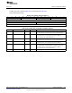
Figure 9-58. FLASH_V Register
31 30 29 28 27 26 25 24 23 22 21 20 19 18 17 16 15 14 13 12 11 10 9 8 7 6 5 4 3 2 1 0
VSL_P VWL_P V_READ RESERVED
R-0h R-0h R-0h R-0h
Table 9-60. FLASH_V Register Field Descriptions
Bit Field Type Reset Description
31-24 VSL_P R 0h
Sourceline voltage applied to the selected block during
programming. Value will be written to FLASH:FVSLP.VSL_P by the
flash device driver when an erase/program operation is initiated.
Reset holds trim value from production test.
23-16 VWL_P R 0h
Wordline voltage applied to the selected half-row during
programming. Value will be written to FLASH:FVWLCT.VWLCT_P
by the flash device driver when an erase/program operation is
initiated.
Reset holds trim value from production test.
15-8 V_READ R 0h
Wordline voltage applied to the selected block during reads and
verifies. Value will be written to FLASH:FVREADCT.VREADCT by
the flash device driver when an erase/program operation is initiated.
Reset holds trim value from production test.
7-0 RESERVED R 0h
Software should not rely on the value of a reserved. Writing any
other value than the reset value may result in undefined behavior.
Reset holds trim value from production test.
752
Device Configuration SWCU117A–February 2015–Revised March 2015
Submit Documentation Feedback
Copyright © 2015, Texas Instruments Incorporated