
User manual


www.ti.com
Factory Configuration (FCFG)
9.2.1.36 FLASH_VHV_PV Register (Offset = 194h) [reset = X]
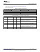
FLASH_VHV_PV is shown in Figure 9-57 and described in Table 9-59.
Flash VHV Program Verify
Figure 9-57. FLASH_VHV_PV Register
31 30 29 28 27 26 25 24 23 22 21 20 19 18 17 16
RESERVED TRIM13_PV RESERVED VHV_PV
R-X R-0h R-X R-8h
15 14 13 12 11 10 9 8 7 6 5 4 3 2 1 0
VCG2P5 VINH
R-0h R-1h
Table 9-59. FLASH_VHV_PV Register Field Descriptions
Bit Field Type Reset Description
31-28 RESERVED R X
Software should not rely on the value of a reserved. Writing any
other value than the reset value may result in undefined behavior.
27-24 TRIM13_PV R 0h
Value will be written to FLASH:FVHVCT1.TRIM13_PV by the flash
device driver when an erase/program operation is initiated.
Reset holds trim value from production test.
23-20 RESERVED R X
Software should not rely on the value of a reserved. Writing any
other value than the reset value may result in undefined behavior.
19-16 VHV_PV R 8h
Value will be written to FLASH:FVHVCT1.VHVCT_PV by the flash
device driver when an erase/program operation is initiated.
15-8 VCG2P5 R 0h
Control gate voltage during read, read margin, and erase verify.
Value will be written to FLASH:FVNVCT.VCG2P5CT by the flash
device driver when an erase/program operation is initiated.
Reset holds trim value from production test.
7-0 VINH R 1h
Inhibit voltage applied to unselected columns during programming.
751
SWCU117A–February 2015–Revised March 2015 Device Configuration
Submit Documentation Feedback
Copyright © 2015, Texas Instruments Incorporated