
User manual


www.ti.com
Factory Configuration (FCFG)
9.2.1.32 FLASH_PP Register (Offset = 184h) [reset = X]
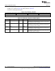
FLASH_PP is shown in Figure 9-53 and described in Table 9-55.
Flash Program Pulse
Figure 9-53. FLASH_PP Register
31 30 29 28 27 26 25 24 23 22 21 20 19 18 17 16 15 14 13 12 11 10 9 8 7 6 5 4 3 2 1 0
PUMP_SU RESERVED MAX_PP
R-X R-0h R-14h
Table 9-55. FLASH_PP Register Field Descriptions
Bit Field Type Reset Description
31-24 PUMP_SU R X
Pump read->non-read mode transition time in half-microseconds
(mainly for FPES).
23-16 RESERVED R 0h
Software should not rely on the value of a reserved. Writing any
other value than the reset value may result in undefined behavior.
Reset holds trim value from production test.
15-0 MAX_PP R 14h
Max program pulse limit per program operation. Value will be written
to FLASH:FSM_PRG_PUL.MAX_PRG_PUL when an erase/program
operation is initiated.
747
SWCU117A–February 2015–Revised March 2015 Device Configuration
Submit Documentation Feedback
Copyright © 2015, Texas Instruments Incorporated