
User manual


www.ti.com
Factory Configuration (FCFG)
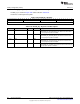
9.2.1.30 FLASH_EH_SEQ Register (Offset = 17Ch) [reset = X]
FLASH_EH_SEQ is shown in Figure 9-51 and described in Table 9-53.
Flash Erase Hold and Sequence
Figure 9-51. FLASH_EH_SEQ Register
31 30 29 28 27 26 25 24 23 22 21 20 19 18 17 16
EH SEQ
R-2h R-X
15 14 13 12 11 10 9 8 7 6 5 4 3 2 1 0
VSTAT SM_FREQUENCY
R-Fh R-X
Table 9-53. FLASH_EH_SEQ Register Field Descriptions
Bit Field Type Reset Description
31-24 EH R 2h
Erase hold time in half-microseconds after SAFELV goes low. Value
will be converted to number of FCLK cycles by the flash device
driver and the converted value is written to
FLASH:FSM_ERA_OH.ERA_OH when an erase/program operation
is initiated.
23-16 SEQ R X
Pump sequence control.
15-12 VSTAT R Fh
Max number of HCLK cycles allowed for pump brown-out. Value will
be written to FLASH:FSM_VSTAT.VSTAT_CNT when an
erase/program operation is initiated.
11-0 SM_FREQUENCY R X
Max FCLK frequency allowed for program, erase, and verify reads.
745
SWCU117A–February 2015–Revised March 2015 Device Configuration
Submit Documentation Feedback
Copyright © 2015, Texas Instruments Incorporated