
User manual


Factory Configuration (FCFG)
www.ti.com
9.2.1 FCFG1 Registers
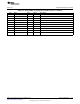
Table 9-23 lists the memory-mapped registers for the FCFG1. All register offset addresses not listed in
Table 9-23 should be considered as reserved locations and the register contents should not be modified.
Table 9-23. FCFG1 Registers
Offset Acronym Register Name Section
C4h CONFIG_RF_FRONTEND_DIV5 Configuration of RF Frontend in Divide-by-5 Mode Section 9.2.1.1
C8h CONFIG_RF_FRONTEND_DIV6 Configuration of RF Frontend in Divide-by-6 Mode Section 9.2.1.2
CCh CONFIG_RF_FRONTEND_DIV10 Configuration of RF Frontend in Divide-by-10 Mode Section 9.2.1.3
D0h CONFIG_RF_FRONTEND_DIV12 Configuration of RF Frontend in Divide-by-12 Mode Section 9.2.1.4
D4h CONFIG_RF_FRONTEND_DIV15 Configuration of RF Frontend in Divide-by-15 Mode Section 9.2.1.5
D8h CONFIG_RF_FRONTEND_DIV30 Configuration of RF Frontend in Divide-by-30 Mode Section 9.2.1.6
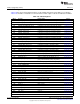
DCh CONFIG_SYNTH_DIV5 Configuration of Synthesizer in Divide-by-5 Mode Section 9.2.1.7
E0h CONFIG_SYNTH_DIV6 Configuration of Synthesizer in Divide-by-6 Mode Section 9.2.1.8
E4h CONFIG_SYNTH_DIV10 Configuration of Synthesizer in Divide-by-10 Mode Section 9.2.1.9
E8h CONFIG_SYNTH_DIV12 Configuration of Synthesizer in Divide-by-12 Mode Section 9.2.1.10
ECh CONFIG_SYNTH_DIV15 Configuration of Synthesizer in Divide-by-15 Mode Section 9.2.1.11
F0h CONFIG_SYNTH_DIV30 Configuration of Synthesizer in Divide-by-30 Mode Section 9.2.1.12
F4h CONFIG_MISC_ADC_DIV5 Configuration of IFADC in Divide-by-5 Mode Section 9.2.1.13
F8h CONFIG_MISC_ADC_DIV6 Configuration of IFADC in Divide-by-6 Mode Section 9.2.1.14
FCh CONFIG_MISC_ADC_DIV10 Configuration of IFADC in Divide-by-10 Mode Section 9.2.1.15
100h CONFIG_MISC_ADC_DIV12 Configuration of IFADC in Divide-by-12 Mode Section 9.2.1.16
104h CONFIG_MISC_ADC_DIV15 Configuration of IFADC in Divide-by-15 Mode Section 9.2.1.17
108h CONFIG_MISC_ADC_DIV30 Configuration of IFADC in Divide-by-30 Mode Section 9.2.1.18
118h SHDW_DIE_ID_0 Shadow of [JTAG_TAP::EFUSE:DIE_ID_0.*] Section 9.2.1.19
11Ch SHDW_DIE_ID_1 Shadow of [JTAG_TAP::EFUSE:DIE_ID_1.*] Section 9.2.1.20
120h SHDW_DIE_ID_2 Shadow of [JTAG_TAP::EFUSE:DIE_ID_2.*] Section 9.2.1.21
124h SHDW_DIE_ID_3 Shadow of [JTAG_TAP::EFUSE:DIE_ID_3.*] Section 9.2.1.22
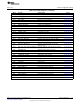
138h SHDW_OSC_BIAS_LDO_TRIM Shadow of Section 9.2.1.23
[JTAG_TAP::EFUSE:OSC_BIAS_LDO_TRIM.*]
13Ch SHDW_ANA_TRIM Shadow of [JTAG_TAP::EFUSE:ANA_TRIM.*] Section 9.2.1.24
164h FLASH_NUMBER Section 9.2.1.25
16Ch FLASH_COORDINATE Section 9.2.1.26
170h FLASH_E_P Flash Erase and Program Setup Time Section 9.2.1.27
174h FLASH_C_E_P_R Flash Compaction, Execute, Program and Read Section 9.2.1.28
178h FLASH_P_R_PV Flash Program, Read, and Program Verify Section 9.2.1.29
17Ch FLASH_EH_SEQ Flash Erase Hold and Sequence Section 9.2.1.30
180h FLASH_VHV_E Flash VHV Erase Section 9.2.1.31
184h FLASH_PP Flash Program Pulse Section 9.2.1.32
188h FLASH_PROG_EP Flash Program and Erase Pulse Section 9.2.1.33
18Ch FLASH_ERA_PW Flash Erase Pulse Width Section 9.2.1.34
190h FLASH_VHV Flash VHV Section 9.2.1.35
194h FLASH_VHV_PV Flash VHV Program Verify Section 9.2.1.36
198h FLASH_V Flash Voltages Section 9.2.1.37
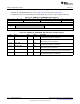
294h USER_ID User Identification Section 9.2.1.38
2B0h FLASH_OTP_DATA3 Flash OTP Data 3 Section 9.2.1.39
2B4h ANA2_TRIM Misc Analog Trim Section 9.2.1.40
2B8h LDO_TRIM LDO Trim Section 9.2.1.41
2E8h MAC_BLE_0 MAC BLE Address 0 Section 9.2.1.42
2ECh MAC_BLE_1 MAC BLE Address 1 Section 9.2.1.43
714
Device Configuration SWCU117A–February 2015–Revised March 2015
Submit Documentation Feedback
Copyright © 2015, Texas Instruments Incorporated