
User manual


www.ti.com
Customer Configuration (CCFG)
9.1.1.13 ERASE_CONF Register (Offset = FDCh) [reset = FFFFFFFFh]
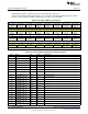
ERASE_CONF is shown in Figure 9-13 and described in Table 9-14.
Erase Configuration
Figure 9-13. ERASE_CONF Register
31 30 29 28 27 26 25 24
RESERVED
R/W-7FFFFFh
23 22 21 20 19 18 17 16
RESERVED
R/W-7FFFFFh
15 14 13 12 11 10 9 8
RESERVED CHIP_ERASE_
DIS_N
R/W-7FFFFFh R/W-1h
7 6 5 4 3 2 1 0
RESERVED BANK_ERASE
_DIS_N
R/W-7Fh R/W-1h
Table 9-14. ERASE_CONF Register Field Descriptions
Bit Field Type Reset Description
31-9 RESERVED R/W 7FFFFFh
Software should not rely on the value of a reserved. Writing any
other value than the reset value may result in undefined behavior.
8 CHIP_ERASE_DIS_N R/W 1h
Chip erase. 0: Disable. Any chip erase request detected during boot
will be ignored. The boot FW will clear
AON_WUC:CTL1.CHIP_ERASE and proceed with normal boot
sequence. 1: Enable. Any chip erase request detected during boot
will be performed by the boot FW.
7-1 RESERVED R/W 7Fh
Software should not rely on the value of a reserved. Writing any
other value than the reset value may result in undefined behavior.
0 BANK_ERASE_DIS_N R/W 1h
Bank erase. This bit will be tested by the ROM boot loader in order
to verify if a received Bank Erase boot loader command can be
executed or not. Bank erase is also referred to as mass erase. 0:
Disable the boot loader bank erase function. 1: Enable the boot
loader bank erase function.
701
SWCU117A–February 2015–Revised March 2015 Device Configuration
Submit Documentation Feedback
Copyright © 2015, Texas Instruments Incorporated