
User manual


Customer Configuration (CCFG)
www.ti.com
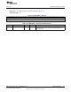
9.1.1.4 VOLT_LOAD_0 Register (Offset = FB8h) [reset = FFFFFFFFh]
VOLT_LOAD_0 is shown in Figure 9-4 and described in Table 9-5.
Voltage Load 0 Enabled by MODE_CONF.VDDR_EXT_LOAD.
Figure 9-4. VOLT_LOAD_0 Register
31 30 29 28 27 26 25 24 23 22 21 20 19 18 17 16
VDDR_EXT_TP45 VDDR_EXT_TP25
R/W-FFh R/W-FFh
15 14 13 12 11 10 9 8 7 6 5 4 3 2 1 0
VDDR_EXT_TP5 VDDR_EXT_TM15
R/W-FFh R/W-FFh
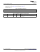
Table 9-5. VOLT_LOAD_0 Register Field Descriptions
Bit Field Type Reset Description
31-24 VDDR_EXT_TP45 R/W FFh
Reserved for future use. Software should not rely on the value of a
reserved. Writing any other value than the reset/default value may
result in undefined behavior.
23-16 VDDR_EXT_TP25 R/W FFh
Reserved for future use. Software should not rely on the value of a
reserved. Writing any other value than the reset/default value may
result in undefined behavior.
15-8 VDDR_EXT_TP5 R/W FFh
Reserved for future use. Software should not rely on the value of a
reserved. Writing any other value than the reset/default value may
result in undefined behavior.
7-0 VDDR_EXT_TM15 R/W FFh
Reserved for future use. Software should not rely on the value of a
reserved. Writing any other value than the reset/default value may
result in undefined behavior.
692
Device Configuration SWCU117A–February 2015–Revised March 2015
Submit Documentation Feedback
Copyright © 2015, Texas Instruments Incorporated