
User manual


www.ti.com
Customer Configuration (CCFG)
9.1.1 CCFG Registers
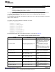
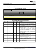
Table 9-1 lists the memory-mapped registers for the CCFG. All register offset addresses not listed in
Table 9-1 should be considered as reserved locations and the register contents should not be modified.
Table 9-1. CCFG Registers
Offset Acronym Register Name Section
FACh MODE_CONF_1 Mode Configuration 1 Section 9.1.1.1
FB0h SIZE_AND_DIS_FLAGS CCFG Size and Disable Flags Section 9.1.1.2
FB4h MODE_CONF Mode Configuration 0 Section 9.1.1.3
FB8h VOLT_LOAD_0 Voltage Load 0 Section 9.1.1.4
FBCh VOLT_LOAD_1 Voltage Load 1 Section 9.1.1.5
FC0h RTC_OFFSET Real Time Clock Offset Section 9.1.1.6
FC4h FREQ_OFFSET Frequency Offset Section 9.1.1.7
FC8h IEEE_MAC_0 IEEE MAC Address 0 Section 9.1.1.8
FCCh IEEE_MAC_1 IEEE MAC Address 1 Section 9.1.1.9
FD0h IEEE_BLE_0 IEEE BLE Address 0 Section 9.1.1.10
FD4h IEEE_BLE_1 IEEE BLE Address 1 Section 9.1.1.11
FD8h BL_CONFIG Bootloader Configuration Section 9.1.1.12
FDCh ERASE_CONF Erase Configuration Section 9.1.1.13
FE0h CCFG_TI_OPTIONS TI Options Section 9.1.1.14
FE4h CCFG_TAP_DAP_0 Test Access Points Enable 0 Section 9.1.1.15
FE8h CCFG_TAP_DAP_1 Test Access Points Enable 1 Section 9.1.1.16
FECh IMAGE_VALID_CONF Image Valid Section 9.1.1.17
FF0h CCFG_PROT_31_0 Protect Sectors 0-31 Section 9.1.1.18
FF4h CCFG_PROT_63_32 Protect Sectors 32-63 Section 9.1.1.19
FF8h CCFG_PROT_95_64 Protect Sectors 64-95 Section 9.1.1.20
FFCh CCFG_PROT_127_96 Protect Sectors 96-127 Section 9.1.1.21
687
SWCU117A–February 2015–Revised March 2015 Device Configuration
Submit Documentation Feedback
Copyright © 2015, Texas Instruments Incorporated