
User manual


www.ti.com
PRCM Registers
6.2.3.8 CTL0 Register (Offset = 20h) [reset = X]
CTL0 is shown in Figure 17-43 and described in Table 17-64.
Control 0 This register contains various chip level control and debug bitfields.
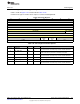
Figure 6-74. CTL0 Register
31 30 29 28 27 26 25 24
RESERVED
R-X
23 22 21 20 19 18 17 16
RESERVED
R-X
15 14 13 12 11 10 9 8
RESERVED PWR_DWN_DI
S
R-X R/W-X
7 6 5 4 3 2 1 0
RESERVED AUX_SRAM_E MCU_SRAM_E RESERVED
RASE RASE
R/W-X W-X W-X R-X
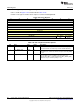
Table 6-78. CTL0 Register Field Descriptions
Bit Field Type Reset Description
31-9 RESERVED R X
Software should not rely on the value of a reserved. Writing any
other value than the reset value may result in undefined behavior.
8 PWR_DWN_DIS R/W X
Controls whether MCU and AUX requesting to be powered off will
enable a transition to powerdown: 0: Enabled 1: Disabled
7-4 RESERVED R/W X
Software should not rely on the value of a reserved. Writing any
other value than the reset value may result in undefined behavior.
3 AUX_SRAM_ERASE W X
Internal. Only to be used through TI provided API.
2 MCU_SRAM_ERASE W X
Internal. Only to be used through TI provided API.
1-0 RESERVED R X
Software should not rely on the value of a reserved. Writing any
other value than the reset value may result in undefined behavior.
501
SWCU117A–February 2015–Revised March 2015 Power, Reset, and Clock Management
Submit Documentation Feedback
Copyright © 2015, Texas Instruments Incorporated