
User manual


Introduction
www.ti.com
6.1.5.2 Active Mode
Active mode is defined as any possible chip state where CPU_PD is powered, including BUS_PD and
VIMS_PD (see Figure 6-2).
In active mode, all modules are available and power consumption is highly application dependent.
Power saving features are:
• Enable the DC-DC converter
• Power only the necessary power domains
• Enable only the necessary module clocks
NOTE: Wake-up time for a power domain in the CC26xx device requires approximately 15 µs.
Because clock gating in the CC26xx device is efficient, it may be more power efficient to
disable all the clocks in a power domain and leave the domain powered may be more power
efficient than to power cycle it frequently.
6.1.5.3 Idle Mode
Idle mode is defined as any possible chip state where CPU_PD is powered off while any other module can
be powered. In idle mode, all modules are available and power consumption is highly application
dependent.
The CC26xx device is put in idle mode with the following requirements:
• [PRCM:PDCTL1.CPU_ON] = 0
• [CPU_SCS:SCR.SLEEPDEEP] = 1
• WFI or WFE active
The CC26xx device may wake up from any wakeup source.
6.1.5.4 Standby Mode
Standby mode is defined as all power domains in the MCU_VD voltage domain being powered off and the
micro LDO supplying AON_VD and MCU_VD (see Figure 6-2). Standby is the lowest power mode where
the CC26xx device still has functionality other than maintaining I/O output pins (see Table 6-6)
All parts in MCU_VD with retention, as shown in Figure 6-3, will be retained in standby mode. All other
logic in MCU_VD needs to be reconfigured after wakeup from Standby mode.
Sensor controller is available in autonomous mode when the CC26xx device is in standby mode.
Possible wake-up sources are events from I/O, JTAG, RTC, and the sensor processor.
The following are prerequisites for the CC26xx device to enter standby mode:
• AUX_PD is powered down or powered off and disconnected from the system bus
• Request micro LDO to supply digital parts (see Figure 6-2)
• JTAG_PD is powered off
• The SCLK_HF clock is derived from the 48-MHz RC oscillator
• The SCLK_LF clock is derived from one of the following clock sources:
– 32-kHz RC oscillator
– 32.768-kHz crystal oscillator
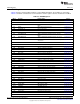
Table 6-6. Example Sequence for Setting CC26xx in Standby Mode
Description Register Required step
Allow for power down [AON_WUC:CTL0.PWR_DWN_DIS] No (Default: Enabled)
Enable the DC-DC converter for [AON_SYSCTL:PWRCTL.DCDC_ACTIVE] No (Default: Global LDO)
lower power
Set the HF clocks to correct source [DDI_0_OSC:CTL0.SCLK_HF_SRC_SEL] Yes
424
Power, Reset, and Clock Management SWCU117A–February 2015–Revised March 2015
Submit Documentation Feedback
Copyright © 2015, Texas Instruments Incorporated