
User manual


ICEPick™
www.ti.com
Table 5-13. Control Block Registers
Register Register Name
0x0 All0s
0x1 Control
0x2 Linking Mode
0x3-0xF Reserved
5.3.4.1.1 All0s Register
This register is a dummy register that returns 0 when read. Writes are ignored. There are not any side
effects to writing or reading this register.
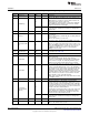
Table 5-14. All0s Register
Bit Field Width Type Reset Description
23-0 Zero 24 R 0 Read zero.
5.3.4.1.2 ICEPick™ Control Register
Table 5-15. ICEPick Control Register
Bit Field Width Type Reset Description
23-7 Reserved 17 RW 0 Reserved
6 BlockSysReset 1 RW 0 When 1, the device system reset signal is blocked.
5-1 Reserved 5 RW 0 Reserved
Emulator controlled System Reset
This signal provides the scan controller with the ability to
assert the system warm reset. When a 1 is written, this
behaves as if the external chip warm reset signal had
0 SystemReset 1 RW 0
been momentarily asserted. This signal does not reset
any emulation logic. This is a self-clearing bit. This is
cleared by the assertion of the reset requested.
Writing a 0 has no effect.
5.3.4.1.3 Linking Mode Register
Table 5-16. ICEPick Linking Mode Register
Bit Field Width Type Reset Description
23-4 Reserved 20 RW 0x0 Reserved
3-1 TAPLinkMode 3 RW 0 See Table 5-17
0 ActivateMode 1 RW 0 When a 1 is written to this bit, the currently selected
TAPLinkMode is activated. ICEPick will link the TAPs
according to these settings when the ICEPick TAP is
advanced to Run‑Test-Idle with any opcode in the IR.
Table 5-17. ICEPick TAP Link Mode
Value Mode Behavior
000 Always-first ICEPick's TAP always exists and is linked as the TAP closest to TDI.
Once activated, the ICEPick TAP is no longer visible between the device
011 Disappear-forever
TDI and TDO. Only a power-on reset will make the TAP visible again.
001-010, 100-111 Reserved Reserved
404
JTAG Interface SWCU117A–February 2015–Revised March 2015
Submit Documentation Feedback
Copyright © 2015, Texas Instruments Incorporated