
User manual


Bit 31 28 27 12 11 1 0
TDI
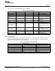
Version Part Number Manufacturer 1
TDO
Access R R R R
Reset VERSION[3:0] PARTNUM[15:0] 000 0001 0111b. 1
Bit 0
TDI
Bypass
TDO
Access RW
Bit 5 0
TDI
Instruction
TDO
Access W
Reset IDCODE
Bit 31 8 7 6 5 1 0
TDI
Bypass
TDO
TDI
Instruction Shift
TDO
TDI
Connection Shift
TDO
TDI
Router or ID Shift
TDO
Access Broad side load and store, serial shift
Reset 0
ICEPick™
www.ti.com
5.3.2.2 Data Shift Register
Figure 5-4 is the register used to shift bits between the ICEPick TDI and TDO. This register is 32 bits
wide. The data shift register has multiple shift in points to facilitate shifts on the instruction path and
several of the data paths.
Figure 5-4. Data Shift Register
When asked to shift, 1-bit is shifted from each bit into the next lower bit. A new value is shifted in from TDI
while the least significant bit is shifted out to TDO. The shift register has several insertion points based on
the current TAP state or value in the instruction register.
5.3.2.3 Instruction Register
This register contains the current TAP instruction. The ICEPick IR is 6 bits wide.
Figure 5-5. Instruction Register
See Table 5-7 for valid IR opcodes.
5.3.2.4 Bypass Register
This register is a 1-bit register. Whatever value is scanned in TDI is preserved and scanned out of TDO
one TCK cycle later.
Figure 5-6. Bypass Register
5.3.2.5 Device Identification Register
This register allows the manufacturer, part number, and version of the device to be determined through
the TAP. The device identification register is scanned in response to the IDCODE instruction.
IDCODE has 3 fields: version, part number, and manufacturer.
Figure 5-7. Device Identification Register
The contents of this register are replicated to a device configuration area which is memory mapped. Refer
to FCFG1:ICEPICK_DEVICE_ID in Section 9.2.1.50 for details of this register.
400
JTAG Interface SWCU117A–February 2015–Revised March 2015
Submit Documentation Feedback
Copyright © 2015, Texas Instruments Incorporated