
User manual


JTAG power domain
Test TAP
PBIST2.0 TAP
WUC
TAP
PBIST1.0 TAP
CPU
I/O
ICEMelter
eFuse TAP
PRCM
TAP
cJTAG
ICEPick
TAP
TCK
TMS
TDO
I/O MUX
2/4pin
Global power reset clock control
/status
TDI/DIO
1149.1
1149.1
1149.1
1149.1
Standby
Wakeup
TDI
MCU voltage domain
AON voltage domain
CPU
/
status
power reset clock control
TDO/DIO
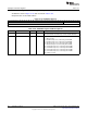
Top Level Debug System
www.ti.com
5.1 Top Level Debug System
The debug subsystem in CC26xx family implements two IEEE standards for debug and test purposes:
• IEEE standard 1149.1: Standard Test Access Port and Boundary Scan Architecture Test Access Port
(TAP) [1]. This standard is known by the acronym JTAG.
• Class 4 IEEE 1149.7: Standard for Reduced-Pin and Enhanced-Functionality Test Access Port and
Boundary-Scan Architecture [2]. This is known by acronym cJTAG (compact JTAG). This standard
serializes the IEEE 1149.1 transactions using a variety of compression formats to reduce the number
of pins needed to implement a JTAG debug port.
The debug subsystem also implements a firewall for unauthorized access to debug/test ports. Figure 5-1
shows a block diagram of debug subsystem.
Figure 5-1. Top Level Debug System
390
JTAG Interface SWCU117A–February 2015–Revised March 2015
Submit Documentation Feedback
Copyright © 2015, Texas Instruments Incorporated