
User manual


BCLK
WCLK
Dx (DSP)A
MSB
LSB
MSB
LSB
MSB
LSB
Channel 0 Channel 1
Channel 2
www.ti.com
Frame Configuration
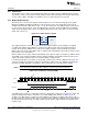
Figure 22-3. DSP Interface Format Example
All samples produced or to be consumed in a sample period must be transferred within a frame, using one
or more data lines. Hence, samples transferred within a frame belong to different audio channels. The
different audio interface formats support a different number of channels per frame; I2S, RJF, and LJF
support one or two channels per frame (one per phase), while DSP supports one to eight channels per
frame. A more detailed description of each supported interface format is presented in Section 22.6, Serial
Interface Formats.
22.3 Frame Configuration
The [I2S:AIFFMTCFG:DUAL_PHASE] register determines the number of phases a frame (one or two). In
the following text, a "WCLK edge" includes the positive edge only for single-phased formats and both
edges for dual-phased formats. A phase is divided into three intervals:
1. DATA DELAY is the inactive period between the WCLK edge and the data period. The duration of this
interval is determined by the [I2S:AIFFMTCFG:DATA_DELAY] register (zero to 255 BCLK cycles). If a
new WCLK edge occurs before the DATA DELAY interval expires, [I2S:IRQFLAGS.WCLK_ERR] is
asserted.
2. WORD is the active period in which a sample word is clocked out or sampled on all ADx pins. The
duration of this interval is determined by [I2S:AIFFMTCFG.WORD_LEN] (8 to 24 BCLK cycles). In
dual-phase mode, the [I2S:IRQFLAGS.WCLK_ERR] register is asserted if two WCLK edges are less
than four BCLK cycles apart. Similar in the single-phase mode, the [I2S:IRQFLAGS.WCLK_ERR]
register will asserted if a new WCLK edge occurs before the last channel is started.
3. IDLE is the inactive period between the last word interval and the next WCLK edge.
22.4 Pin Configuration
The ADx pins can be individually configured to be input, output or not in use by setting the
[I2S:AIFDIRCFG:AD0], [I2S:AIFDIRCFG:AD1] and [I2S:AIFDIRCFG:AD2] registers as:
• 0x0: Not in use
• 0x1: Input
• 0x2: Output
When a direction is completely unused, there is no need to configure the corresponding memory access
and sample stamp registers. The ADx pins, together with the clock pins, are configured in the I/O
controller.
22.5 Clock Configuration
The I2S module includes one clock control register, [I2S:AIFWCLKSRC]; all other I2S clock configurations
are done in the PRCM module.
The [I2S:AIFWCLKSRC:WCLK_SRC] register selects an internal or external WCLK source for the I2S
module. The selected source should be the same as the BCLK source selected in the
[PRCM:I2SBCLKSEL:SRC] register. The WCLK source (internal or external) can be inverted using the
[I2S:AIFWCLKSRC:WCLK_INV] register. For example, the inverted WCLK source is used for the I2S
serial interface format.
1413
SWCU117A–February 2015–Revised March 2015 Integrated Interchip Sound (I2S) Module
Submit Documentation Feedback
Copyright © 2015, Texas Instruments Incorporated