
User manual


SSI Registers
www.ti.com
20.7.1.3 DR Register (Offset = 8h) [reset = X]
DR is shown in Figure 20-15 and described in Table 20-5.
Data 16-bits wide data register: When read, the entry in the receive FIFO, pointed to by the current FIFO
read pointer, is accessed. As data values are removed by the receive logic from the incoming data frame,
they are placed into the entry in the receive FIFO, pointed to by the current FIFO write pointer. When
written, the entry in the transmit FIFO, pointed to by the write pointer, is written to. Data values are
removed from the transmit FIFO one value at a time by the transmit logic. It is loaded into the transmit
serial shifter, then serially shifted out onto the TXD output pin at the programmed bit rate. When a data
size of less than 16 bits is selected, the user must right-justify data written to the transmit FIFO. The
transmit logic ignores the unused bits. Received data less than 16 bits is automatically right-justified in the
receive buffer.
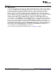
Figure 20-15. DR Register
31 30 29 28 27 26 25 24 23 22 21 20 19 18 17 16 15 14 13 12 11 10 9 8 7 6 5 4 3 2 1 0
RESERVED DATA
R-X R/W-0h
Table 20-5. DR Register Field Descriptions
Bit Field Type Reset Description
31-16 RESERVED R X
Software should not rely on the value of a reserved. Writing any
other value than the reset value may result in undefined behavior.
15-0 DATA R/W 0h
Transmit/receive data The values read from this field or written to
this field must be right-justified when SSI is programmed for a data
size that is less than 16 bits (CR0.DSS != 0b1111). Unused bits at
the top are ignored by transmit logic. The receive logic automatically
right-justifies.
1370
Synchronous Serial Interface (SSI) SWCU117A–February 2015–Revised March 2015
Submit Documentation Feedback
Copyright © 2015, Texas Instruments Incorporated