
User manual


LSB
SSIn_Clk
SSIn_Fss
SSIn_Tx/SSIn_Rx
4 to 16 bits
SSIn_Clk
SSIn_Fss
SSIn_Tx/SSIn_Rx
MSB LSB
4 to 16 bits
Functional Description
www.ti.com
20.4.4 Frame Formats
Each data frame is between 4 and 16 bits long, depending on the size of data programmed, and is
transmitted starting with the most significant bit (MSB). Three basic frame types can be selected:
• TI synchronous serial
• Motorola SPI
• National MICROWIRE
For all three formats, the serial clock (SSIn_CLK) is held inactive while the SSI is idle and SSIn_CLK
transitions at the programmed frequency only during active transmission or reception of data. The IDLE
state of SSIn_CLK provides a receive time-out indication that occurs when the RX FIFO still contains data
after a time-out period.
For Motorola SPI and MICROWIRE frame formats, the serial frame (SSIn_FSS) pin is active low and is
asserted (pulled down) during the entire transmission of the frame.
For TI synchronous serial frame format, the SSIn_FSS pin is pulsed for one serial clock period which
starts at its rising edge before the transmission of each frame. For this frame format, both the SSI and the
off-chip slave device drive their output data on the rising edge of SSIn_CLK and latch data from the other
device on the falling edge.
Unlike the full-duplex transmission of the other two frame formats, the MICROWIRE format uses a special
master-slave messaging technique that operates at half-duplex. When a frame begins, an 8-bit control
message is transmitted to the off-chip slave. No incoming data is received by the SSI during this
transmission. After the message is sent, the off-chip slave decodes it and responds with the requested
data after waiting one serial clock after the last bit of the 8-bit control message is sent. The returned data
can be 4 to 16 bits long, making the total frame length anywhere from 13 to 25 bits.
20.4.4.1 Texas Instruments Synchronous Serial Frame Format
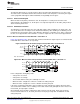
Figure 20-2 shows the TI synchronous serial frame format for a single transmitted frame.
Figure 20-2. TI Synchronous Serial Frame Format (Single Transfer)
SSIn_CLK and SSIn_FSS are forced low and the transmit data line SSIn_TX is tristated whenever the SSI
is idle. When the bottom entry of the TX FIFO contains data, SSIn_FSS is pulsed high for one SSIn_CLK
period. The transmitted value is also transferred from the TX FIFO to the serial shift register of the
transmit logic. On the next rising edge of SSIn_CLK, the MSB of the 4- to 16-bit data frame is shifted out
on the SSIn_TX pin. Likewise, the MSB of the received data is shifted onto the SSIn_RX pin by the off-
chip serial slave device.
Both the SSI and the off-chip serial slave device then clock each data bit into their serial shifter on each
falling edge of SSIn_CLK. The received data is transferred from the serial shifter to the RX FIFO on the
first rising edge of SSIn_CLK after the least significant bit (LSB) is latched.
Figure 20-3 shows the TI synchronous serial frame format when back-to-back frames are transmitted.
Figure 20-3. TI Synchronous Serial Frame Format (Continuous Transfer)
1358
Synchronous Serial Interface (SSI) SWCU117A–February 2015–Revised March 2015
Submit Documentation Feedback
Copyright © 2015, Texas Instruments Incorporated