
User manual


Cortex-M3 Processor Registers
www.ti.com
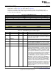
2.7.2.17 FUNCTION2 Register (Offset = 48h) [reset = X]
FUNCTION2 is shown in Figure 2-57 and described in Table 2-81.
Function 2 Use the DWT Function Registers 2 to control the operation of the comparator 2. This
comparator can emit data or PC couples, trigger the ETM, or generate a watchpoint depending on the
operation defined by FUNCTION.
Figure 2-57. FUNCTION2 Register
31 30 29 28 27 26 25 24
RESERVED MATCHED
R/W-X R/W-X
23 22 21 20 19 18 17 16
RESERVED
R-X
15 14 13 12 11 10 9 8
RESERVED
R-X
7 6 5 4 3 2 1 0
RESERVED EMITRANGE RESERVED FUNCTION
R-X R/W-X R-X R/W-X
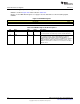
Table 2-81. FUNCTION2 Register Field Descriptions
Bit Field Type Reset Description
31-25 RESERVED R/W X
Software should not rely on the value of a reserved. Writing any
other value than the reset value may result in undefined behavior.
24 MATCHED R/W X
This bit is set when the comparator matches, and indicates that the
operation defined by FUNCTION has occurred since this bit was last
read. This bit is cleared on read.
23-6 RESERVED R X
Software should not rely on the value of a reserved. Writing any
other value than the reset value may result in undefined behavior.
5 EMITRANGE R/W X
Emit range field. This bit permits emitting offset when range match
occurs. PC sampling is not supported when emit range is enabled.
This field only applies for: FUNCTION = 1, 2, 3, 12, 13, 14, and 15.
4 RESERVED R X
Software should not rely on the value of a reserved. Writing any
other value than the reset value may result in undefined behavior.
3-0 FUNCTION R/W X
Function settings. 0x0: Disabled 0x1: EMITRANGE = 0, sample and
emit PC through ITM. EMITRANGE = 1, emit address offset through
ITM 0x2: EMITRANGE = 0, emit data through ITM on read and write.
EMITRANGE = 1, emit data and address offset through ITM on read
or write. 0x3: EMITRANGE = 0, sample PC and data value through
ITM on read or write. EMITRANGE = 1, emit address offset and data
value through ITM on read or write. 0x4: Watchpoint on PC match.
0x5: Watchpoint on read. 0x6: Watchpoint on write. 0x7: Watchpoint
on read or write. 0x8: ETM trigger on PC match 0x9: ETM trigger on
read 0xA: ETM trigger on write 0xB: ETM trigger on read or write
0xC: EMITRANGE = 0, sample data for read transfers. EMITRANGE
= 1, sample Daddr (lower 16 bits) for read transfers 0xD:
EMITRANGE = 0, sample data for write transfers. EMITRANGE = 1,
sample Daddr (lower 16 bits) for write transfers 0xE: EMITRANGE =
0, sample PC + data for read transfers. EMITRANGE = 1, sample
Daddr (lower 16 bits) + data for read transfers 0xF: EMITRANGE =
0, sample PC + data for write transfers. EMITRANGE = 1, sample
Daddr (lower 16 bits) + data for write transfers Note 1: If the ETM is
not fitted, then ETM trigger is not possible. Note 2: Data value is only
sampled for accesses that do not fault (MPU or bus fault). The PC is
sampled irrespective of any faults. The PC is only sampled for the
first address of a burst. Note 3: PC match is not recommended for
watchpoints because it stops after the instruction. It mainly guards
and triggers the ETM.
112
SWCU117A–February 2015–Revised March 2015
Submit Documentation Feedback
Copyright © 2015, Texas Instruments Incorporated