
User manual


www.ti.com
Cortex-M3 Processor Registers
2.7.2.10 MASK0 Register (Offset = 24h) [reset = X]
MASK0 is shown in Figure 2-50 and described in Table 2-74.
Mask 0 Use the DWT Mask Registers 0 to apply a mask to data addresses when matching against
COMP0.
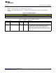
Figure 2-50. MASK0 Register
31 30 29 28 27 26 25 24 23 22 21 20 19 18 17 16 15 14 13 12 11 10 9 8 7 6 5 4 3 2 1 0
RESERVED MASK
R/W-X R/W-0h
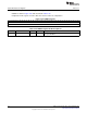
Table 2-74. MASK0 Register Field Descriptions
Bit Field Type Reset Description
31-4 RESERVED R/W X
Software should not rely on the value of a reserved. Writing any
other value than the reset value may result in undefined behavior.
3-0 MASK R/W 0h
Mask on data address when matching against COMP0. This is the
size of the ignore mask. That is, DWT matching is performed
as:(ADDR ANDed with (0xFFFF left bit-shifted by MASK)) ==
COMP0. However, the actual comparison is slightly more complex to
enable matching an address wherever it appears on a bus. So, if
COMP0 is 3, this matches a word access of 0, because 3 would be
within the word.
103
SWCU117A–February 2015–Revised March 2015
Submit Documentation Feedback
Copyright © 2015, Texas Instruments Incorporated