
User manual


I/O Control Registers
www.ti.com
11.11.3 GPIO Registers
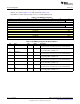
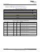
Table 11-43 lists the memory-mapped registers for the GPIO. All register offset addresses not listed in
Table 11-43 should be considered as reserved locations and the register contents should not be modified.
Table 11-43. GPIO Registers
Offset Acronym Register Name Section
0h DOUT3_0 Data Out 0 to 3 Section 11.11.3.1
4h DOUT7_4 Data Out 4 to 7 Section 11.11.3.2
8h DOUT11_8 Data Out 8 to 11 Section 11.11.3.3
Ch DOUT15_12 Data Out 12 to 15 Section 11.11.3.4
10h DOUT19_16 Data Out 16 to 19 Section 11.11.3.5
14h DOUT23_20 Data Out 20 to 23 Section 11.11.3.6
18h DOUT27_24 Data Out 24 to 27 Section 11.11.3.7
1Ch DOUT31_28 Data Out 28 to 31 Section 11.11.3.8
80h DOUT31_0 Data Output for DIO 0 to 31 Section 11.11.3.9
90h DOUTSET31_0 Data Out Set Section 11.11.3.10
A0h DOUTCLR31_0 Data Out Clear Section 11.11.3.11
B0h DOUTTGL31_0 Data Out Toggle Section 11.11.3.12
C0h DIN31_0 Data Input from DIO 0 to 31 Section 11.11.3.13
D0h DOE31_0 Data Output Enable for DIO 0 to 31 Section 11.11.3.14
E0h EVFLAGS31_0 Event Register for DIO 0 to 31 Section 11.11.3.15
1012
I/O Control SWCU117A–February 2015–Revised March 2015
Submit Documentation Feedback
Copyright © 2015, Texas Instruments Incorporated