
User's Manual
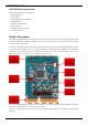
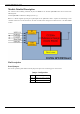
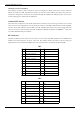
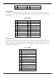
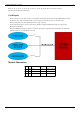

Table Of Contents

CC256x QFN EM User Guide
5
17 MODULE_AUDIO_CLK 18 MODULE_UART_RTS
19 WCS_NSHUTD 20 N/C
Debug Header
The debug header is provided for testing and debugging purposes. It exposes important signals used in the design
such as power, ground, debug, UART, and Audio signals. Note that all I/O's are at 1.8V. Pinout is shown in the
following table:
DEBUG HDR
Pin # EM Adapter Pin Assignment Pin€# EM Adapter Pin Assignment
1 GND 2 VBAT
3 VIO_HOST 4 GND
5 AUD_FSYNC_1V8 6 AUD_CLK_1V8
7 AUD_OUT_1V8 8 AUD_IN_1V8
9 CLK_REQ_OUT_1V8 10 SLOW_CLK_EDGE
11 HCI_TX_1V8 12 HCI_RX_1V8
13 HCI_CTS_1V8 14 HCI_RTS_1V8
15 TX_DEBUG_1V8 16 nSHUTDOWN_1V8
17 VDD_1V8 18 GND
COM Connector
The COM connector, aka Edge card, is used to interface with TI's MPUs such as OMAP and AM335x. As shown
below, it provides HCI, Audio, Slow Clock, Shutdown, and Debug interfaces to the host connected through the edge
card. Note that all I/O's for the COM connector are at 1.8V. Also note some components should be DNI to use the
COM connector. See BOM for details.
COM€CARD
Pin # Relevant COM Connector Pin Assignment
1 SLOW_CLK_EDGE
8 1V8_IN
52 AUD_CLK_1V8
54 AUD_FSYNC_1V8
56 AUD_IN_1V8
58 AUD_OUT_1V8
66 HCI_TX_1V8
68 HCI_RX_1V8
70 HCI_CTS_1V8
72 HCI_RTS_1V8
76 TX_DEBUG_1V8
89 nSHUTDOWN_1V8