
User manual
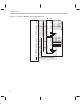
Table Of Contents
- Read This First
- Contents
- Figures
- Tables
- Examples
- Cautions
- Introduction
- Architectural Overview
- Central Processing Unit
- Memory and I/O Spaces
- Program Control
- Addressing Modes
- Assembly Language Instructions
- Instruction Set Summary
- How To Use the Instruction Descriptions
- Instruction Descriptions
- ABS
- ABS
- ADD
- ADD
- ADD
- ADD
- ADDC
- ADDC
- ADDS
- ADDS
- ADDT
- ADDT
- ADRK
- AND
- AND
- AND
- APAC
- APAC
- B
- BACC
- BANZ
- BANZ
- BCND
- BCND
- BIT
- BIT
- BITT
- BITT
- BLDD
- BLDD
- BLDD
- BLDD
- BLDD
- BLPD
- BLPD
- BLPD
- BLPD
- CALA
- CALL
- CC
- CC
- CLRC
- CLRC
- CMPL
- CMPR
- DMOV
- DMOV
- IDLE
- IN
- IN
- INTR
- LACC
- LACC
- LACC
- LACL
- LACL
- LACL
- LACT
- LACT
- LAR
- LAR
- LAR
- LDP
- LDP
- LPH
- LPH
- LST
- LST
- LST
- LST
- LT
- LT
- LTA
- LTA
- LTD
- LTD
- LTD
- LTP
- LTP
- LTS
- LTS
- MAC
- MAC
- MAC
- MAC
- MACD
- MACD
- MACD
- MACD
- MACD
- MAR
- MAR
- MPY
- MPY
- MPY
- MPYA
- MPYA
- MPYS
- MPYS
- MPYU
- MPYU
- NEG
- NEG
- NMI
- NOP
- NORM
- NORM
- NORM
- OR
- OR
- OR
- OUT
- OUT
- PAC
- POP
- POP
- POPD
- POPD
- PSHD
- PSHD
- PUSH
- RET
- RETC
- ROL
- ROR
- RPT
- RPT
- SACH
- SACH
- SACL
- SACL
- SAR
- SAR
- SBRK
- SETC
- SETC
- SFL
- SFR
- SFR
- SPAC
- SPH
- SPH
- SPL
- SPL
- SPLK
- SPLK
- SPM
- SQRA
- SQRA
- SQRS
- SQRS
- SST
- SST
- SUB
- SUB
- SUB
- SUB
- SUBB
- SUBB
- SUBC
- SUBC
- SUBS
- SUBS
- SUBT
- SUBT
- TBLR
- TBLR
- TBLR
- TBLW
- TBLW
- TBLW
- TRAP
- XOR
- XOR
- XOR
- ZALR
- ZALR
- On-Chip Peripherals
- Synchronous Serial Port
- Asynchronous Serial Port
- TMS320C209
- Register Summary
- TMS320C1x/C2x/C2xx/C5x Instruction Set Comparison
- Program Examples
- Submitting ROM Codes to TI
- Design Considerations for Using XDS510 Emulator
- E.1 Designing Your Target System’s Emulator Connector (14-Pin Header)
- E.2 Bus Protocol
- E.3 Emulator Cable Pod
- E.4 Emulator Cable Pod Signal Timing
- E.5 Emulation Timing Calculations
- E.6 Connections Between the Emulator and the Target System
- E.7 Physical Dimensions for the 14-Pin Emulator Connector
- E.8 Emulation Design Considerations
- Glossary
- Index
Overview of the Memory and I/O Spaces
4-3
Memory and I/O Spaces
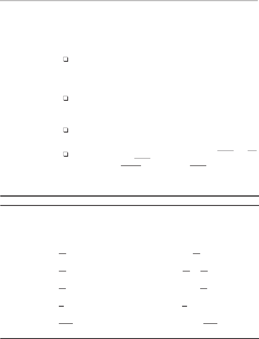
4.1.1 Pins for Interfacing to External Memory and I/O Spaces
The pins for interfacing to external memory and I/O space, described in
Table 4–1, are of four main types:
External buses. Sixteen signals (A15–A0) are available for passing an
address from the ’C2xx to another device. Sixteen signals (D15–D0) are
available for transferring a data value between the ’C2xx and another de-
vice.
Select signals. These signals can be used by external devices to deter-
mine when the ’C2xx is requesting access to off-chip locations, and
whether that request is for data, program, global, or I/O space.
Read/write signals. These signals indicate to external devices the direc-
tion of a data transfer (to the ’C2xx or from the ’C2xx).
Request/control signals. The input request signals (BOOT, MP/MC,
RAMEN, READY, and HOLD
) effect a change in the operation of the
’C2xx. The output HOLDA
is the response to HOLD.
Table 4–1. Pins for Interfacing With External Memory and I/O Spaces
Pin(s) Description
External buses A15–A0 The 16 lines of the external address bus. This bus can address up to 64K
words of external memory or I/O space.
D15–D0 The 16 bidirectional lines of the external data bus. This bus carries data
to and from external memory or I/O space.
Select signals DS
Data memory select pin. The ’C2xx asserts DS to indicate an access to
external data memory (local or global).
BR
Bus request pin. The ’C2xx asserts both BR and DS to indicate an access
to global data memory.
PS
Program memory select pin. The ’C2xx asserts PS to indicate an access
to external program memory.
IS
I/O space select pin. The ’C2xx asserts IS to indicate an access to exter-
nal I/O space.
STRB External access active strobe. The ’C2xx asserts STRB during accesses
to external program, data, or I/O space.