
User manual
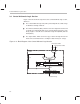
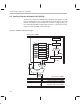
Table Of Contents
- Read This First
- Contents
- Figures
- Tables
- Examples
- Cautions
- Introduction
- Architectural Overview
- Central Processing Unit
- Memory and I/O Spaces
- Program Control
- Addressing Modes
- Assembly Language Instructions
- Instruction Set Summary
- How To Use the Instruction Descriptions
- Instruction Descriptions
- ABS
- ABS
- ADD
- ADD
- ADD
- ADD
- ADDC
- ADDC
- ADDS
- ADDS
- ADDT
- ADDT
- ADRK
- AND
- AND
- AND
- APAC
- APAC
- B
- BACC
- BANZ
- BANZ
- BCND
- BCND
- BIT
- BIT
- BITT
- BITT
- BLDD
- BLDD
- BLDD
- BLDD
- BLDD
- BLPD
- BLPD
- BLPD
- BLPD
- CALA
- CALL
- CC
- CC
- CLRC
- CLRC
- CMPL
- CMPR
- DMOV
- DMOV
- IDLE
- IN
- IN
- INTR
- LACC
- LACC
- LACC
- LACL
- LACL
- LACL
- LACT
- LACT
- LAR
- LAR
- LAR
- LDP
- LDP
- LPH
- LPH
- LST
- LST
- LST
- LST
- LT
- LT
- LTA
- LTA
- LTD
- LTD
- LTD
- LTP
- LTP
- LTS
- LTS
- MAC
- MAC
- MAC
- MAC
- MACD
- MACD
- MACD
- MACD
- MACD
- MAR
- MAR
- MPY
- MPY
- MPY
- MPYA
- MPYA
- MPYS
- MPYS
- MPYU
- MPYU
- NEG
- NEG
- NMI
- NOP
- NORM
- NORM
- NORM
- OR
- OR
- OR
- OUT
- OUT
- PAC
- POP
- POP
- POPD
- POPD
- PSHD
- PSHD
- PUSH
- RET
- RETC
- ROL
- ROR
- RPT
- RPT
- SACH
- SACH
- SACL
- SACL
- SAR
- SAR
- SBRK
- SETC
- SETC
- SFL
- SFR
- SFR
- SPAC
- SPH
- SPH
- SPL
- SPL
- SPLK
- SPLK
- SPM
- SQRA
- SQRA
- SQRS
- SQRS
- SST
- SST
- SUB
- SUB
- SUB
- SUB
- SUBB
- SUBB
- SUBC
- SUBC
- SUBS
- SUBS
- SUBT
- SUBT
- TBLR
- TBLR
- TBLR
- TBLW
- TBLW
- TBLW
- TRAP
- XOR
- XOR
- XOR
- ZALR
- ZALR
- On-Chip Peripherals
- Synchronous Serial Port
- Asynchronous Serial Port
- TMS320C209
- Register Summary
- TMS320C1x/C2x/C2xx/C5x Instruction Set Comparison
- Program Examples
- Submitting ROM Codes to TI
- Design Considerations for Using XDS510 Emulator
- E.1 Designing Your Target System’s Emulator Connector (14-Pin Header)
- E.2 Bus Protocol
- E.3 Emulator Cable Pod
- E.4 Emulator Cable Pod Signal Timing
- E.5 Emulation Timing Calculations
- E.6 Connections Between the Emulator and the Target System
- E.7 Physical Dimensions for the 14-Pin Emulator Connector
- E.8 Emulation Design Considerations
- Glossary
- Index
Status Registers ST0 and ST1
3-15
Central Processing Unit
3.5 Status Registers ST0 and ST1
The ’C2xx has two status registers, ST0 and ST1, which contain status and
control bits. These registers can be stored into and loaded from data memory,
thus allowing the status of the machine to be saved and restored for subrou-
tines.
The LST (load status register) instruction writes to ST0 and ST1, and the SST
(store status register) instruction reads from ST0 and ST1 (with the exception
of the INTM bit, which is not affected by the LST instruction). Many of the indi-
vidual bits of these registers can be set and cleared using the SETC and CLRC
instructions. For example, the sign-extension mode is set with SETC SXM and
cleared with CLRC SXM.
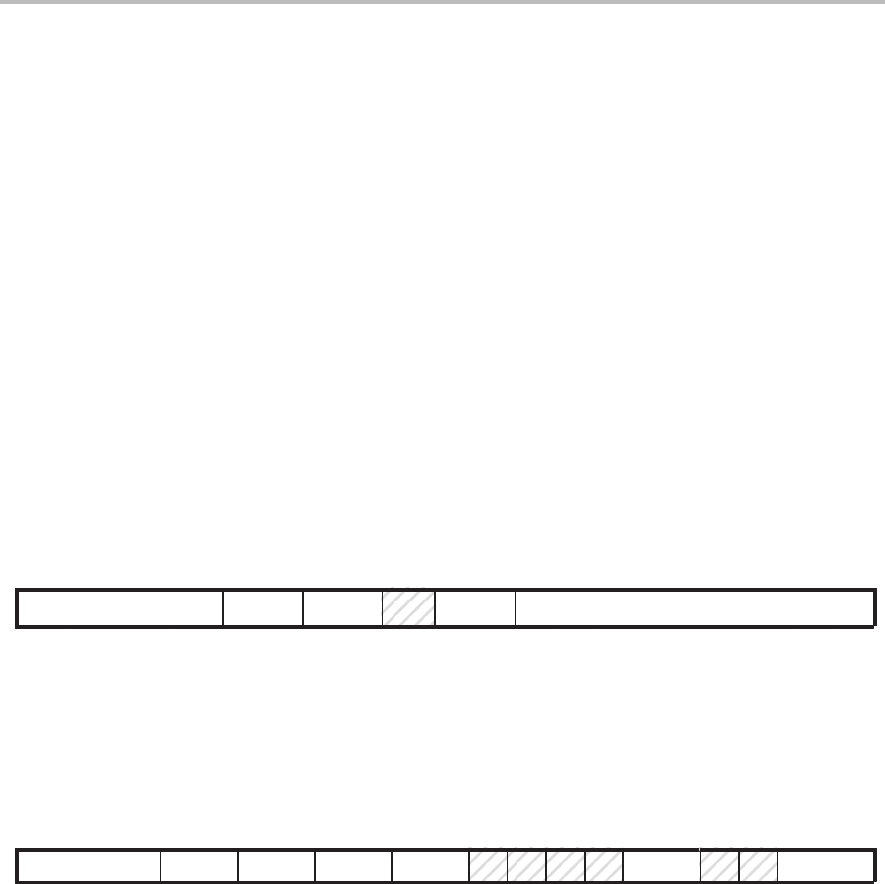
Figure 3–10 and Figure 3–11 show the organization of status registers ST0
and ST1, respectively. Several bits in the status registers are reserved; they
are always read as logic 1s. The other bits are described in alphabetical order
in Table 3–2.
Figure 3–10. Status Register ST0
15 14 13 12 11 10 9 8 7 6 5 4 3 2 1 0
ARP OV OVM 1
†
INTM DP
R/W–x R/W–0 R/W–x R/W–1 R/W–x
Note: R = Read access; W = Write access; value following dash (–) is value after reset (x means value not affected by
reset).
†
This reserved bit is always read as 1. Writes have no effect on it.
Figure 3–11.Status Register ST1
151413 12 11 10 9 8765 4 32 1 0
ARB CNF TC SXM C 1
†
1
†
1
†
1
†
XF 1
†
1
†
PM
R/W–x R/W–0 R/W–x R/W–1 R/W–1 R/W–1 R/W–00
Note: R = Read access; W = Write access; value following dash (–) is value after reset (x means value not affected by
reset).
†
These reserved bits are always read as 1s. Writes have no effect on them.