
User manual
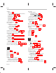
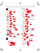
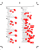
Table Of Contents
- Read This First
- Contents
- Figures
- Tables
- Examples
- Cautions
- Introduction
- Architectural Overview
- Central Processing Unit
- Memory and I/O Spaces
- Program Control
- Addressing Modes
- Assembly Language Instructions
- Instruction Set Summary
- How To Use the Instruction Descriptions
- Instruction Descriptions
- ABS
- ABS
- ADD
- ADD
- ADD
- ADD
- ADDC
- ADDC
- ADDS
- ADDS
- ADDT
- ADDT
- ADRK
- AND
- AND
- AND
- APAC
- APAC
- B
- BACC
- BANZ
- BANZ
- BCND
- BCND
- BIT
- BIT
- BITT
- BITT
- BLDD
- BLDD
- BLDD
- BLDD
- BLDD
- BLPD
- BLPD
- BLPD
- BLPD
- CALA
- CALL
- CC
- CC
- CLRC
- CLRC
- CMPL
- CMPR
- DMOV
- DMOV
- IDLE
- IN
- IN
- INTR
- LACC
- LACC
- LACC
- LACL
- LACL
- LACL
- LACT
- LACT
- LAR
- LAR
- LAR
- LDP
- LDP
- LPH
- LPH
- LST
- LST
- LST
- LST
- LT
- LT
- LTA
- LTA
- LTD
- LTD
- LTD
- LTP
- LTP
- LTS
- LTS
- MAC
- MAC
- MAC
- MAC
- MACD
- MACD
- MACD
- MACD
- MACD
- MAR
- MAR
- MPY
- MPY
- MPY
- MPYA
- MPYA
- MPYS
- MPYS
- MPYU
- MPYU
- NEG
- NEG
- NMI
- NOP
- NORM
- NORM
- NORM
- OR
- OR
- OR
- OUT
- OUT
- PAC
- POP
- POP
- POPD
- POPD
- PSHD
- PSHD
- PUSH
- RET
- RETC
- ROL
- ROR
- RPT
- RPT
- SACH
- SACH
- SACL
- SACL
- SAR
- SAR
- SBRK
- SETC
- SETC
- SFL
- SFR
- SFR
- SPAC
- SPH
- SPH
- SPL
- SPL
- SPLK
- SPLK
- SPM
- SQRA
- SQRA
- SQRS
- SQRS
- SST
- SST
- SUB
- SUB
- SUB
- SUB
- SUBB
- SUBB
- SUBC
- SUBC
- SUBS
- SUBS
- SUBT
- SUBT
- TBLR
- TBLR
- TBLR
- TBLW
- TBLW
- TBLW
- TRAP
- XOR
- XOR
- XOR
- ZALR
- ZALR
- On-Chip Peripherals
- Synchronous Serial Port
- Asynchronous Serial Port
- TMS320C209
- Register Summary
- TMS320C1x/C2x/C2xx/C5x Instruction Set Comparison
- Program Examples
- Submitting ROM Codes to TI
- Design Considerations for Using XDS510 Emulator
- E.1 Designing Your Target System’s Emulator Connector (14-Pin Header)
- E.2 Bus Protocol
- E.3 Emulator Cable Pod
- E.4 Emulator Cable Pod Signal Timing
- E.5 Emulation Timing Calculations
- E.6 Connections Between the Emulator and the Target System
- E.7 Physical Dimensions for the 14-Pin Emulator Connector
- E.8 Emulation Design Considerations
- Glossary
- Index

Index
Index-13
L
LACC instruction 7-72
LACL instruction 7-75
LACT instruction 7-78
LAR instruction 7-80
latch phase of CPU cycle F-13
latency, interrupt 5-30 to 5-36
after execution of RET 5-32
during execution of CLRC INTM 5-31
minimum latency 5-30
LDP instruction 7-83
local data memory
address map
’C203 4-32
’C204 4-35
’C209 11-6
configuration
RAM (dual-access)
’C203 4-33
’C204 4-36
’C209 11-8
RAM (single-access) 11-7
description 4-7
external interfacing 4-9
caution about proper timing 4-9
pages of (diagram) 4-7
logic instructions
AND 7-34
CMPL (complement/NOT) 7-64
OR 7-129
XOR (exclusive OR) 7-193
logic phase of CPU cycle F-13
long immediate addressing 6-2
LPH instruction 7-85
LST instruction 7-87
LT instruction 7-91
LTA instruction 7-93
LTD instruction 7-95
LTP instruction 7-98
LTS instruction 7-100
M
MAC instruction 7-102
MACD instruction 7-106
MAR instruction 7-111
mask bits
asynchronous serial port control register
(ASPCR) 10-8
interrupt control register (ICR) 5-24
interrupt mask register (IMR) 5-22
maskable interrupts 5-18
acknowledgement conditions 5-19
definition 5-15
enabling/disabling with INTM bit 5-19
flag bits in ICR 5-24
flag bits in IFR 5-20
flow chart of operation 5-20
flow chart of requesting INT2
and INT3 5-18
masking/unmasking in ICR 5-24
masking/unmasking in IMR 5-22
MCM bit 9-11
memory
See also
I/O space
address map
’C203 4-32
’C204 4-35
’C209 11-6
data page 0 4-8
available on TMS320C2xx devices 2-7
available types 1-6
boot loader 4-14
boot source (EPROM) 4-14
diagram 4-14
enabling 4-17
execution 4-18
generating code for EPROM C-23 to C-24
program code 4-21
data page pointer (DP) 3-16
device-specific information 4-31
direct memory access (using HOLD opera-
tion) 4-27
during reset 4-29
example 4-28
terminating correctly 4-29
external interfacing
global data memory 4-12
I/O ports 4-25
local data memory 4-9
program memory 4-5
flash, introduction 2-9
global data memory 4-11 to 4-13
HOLD operation 4-27 to 4-30
during reset 4-29
example 4-28
terminating correctly 4-29