
User manual
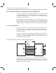
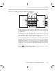
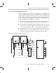
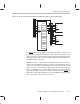
Table Of Contents
- Read This First
- Contents
- Figures
- Tables
- Examples
- Cautions
- Introduction
- Architectural Overview
- Central Processing Unit
- Memory and I/O Spaces
- Program Control
- Addressing Modes
- Assembly Language Instructions
- Instruction Set Summary
- How To Use the Instruction Descriptions
- Instruction Descriptions
- ABS
- ABS
- ADD
- ADD
- ADD
- ADD
- ADDC
- ADDC
- ADDS
- ADDS
- ADDT
- ADDT
- ADRK
- AND
- AND
- AND
- APAC
- APAC
- B
- BACC
- BANZ
- BANZ
- BCND
- BCND
- BIT
- BIT
- BITT
- BITT
- BLDD
- BLDD
- BLDD
- BLDD
- BLDD
- BLPD
- BLPD
- BLPD
- BLPD
- CALA
- CALL
- CC
- CC
- CLRC
- CLRC
- CMPL
- CMPR
- DMOV
- DMOV
- IDLE
- IN
- IN
- INTR
- LACC
- LACC
- LACC
- LACL
- LACL
- LACL
- LACT
- LACT
- LAR
- LAR
- LAR
- LDP
- LDP
- LPH
- LPH
- LST
- LST
- LST
- LST
- LT
- LT
- LTA
- LTA
- LTD
- LTD
- LTD
- LTP
- LTP
- LTS
- LTS
- MAC
- MAC
- MAC
- MAC
- MACD
- MACD
- MACD
- MACD
- MACD
- MAR
- MAR
- MPY
- MPY
- MPY
- MPYA
- MPYA
- MPYS
- MPYS
- MPYU
- MPYU
- NEG
- NEG
- NMI
- NOP
- NORM
- NORM
- NORM
- OR
- OR
- OR
- OUT
- OUT
- PAC
- POP
- POP
- POPD
- POPD
- PSHD
- PSHD
- PUSH
- RET
- RETC
- ROL
- ROR
- RPT
- RPT
- SACH
- SACH
- SACL
- SACL
- SAR
- SAR
- SBRK
- SETC
- SETC
- SFL
- SFR
- SFR
- SPAC
- SPH
- SPH
- SPL
- SPL
- SPLK
- SPLK
- SPM
- SQRA
- SQRA
- SQRS
- SQRS
- SST
- SST
- SUB
- SUB
- SUB
- SUB
- SUBB
- SUBB
- SUBC
- SUBC
- SUBS
- SUBS
- SUBT
- SUBT
- TBLR
- TBLR
- TBLR
- TBLW
- TBLW
- TBLW
- TRAP
- XOR
- XOR
- XOR
- ZALR
- ZALR
- On-Chip Peripherals
- Synchronous Serial Port
- Asynchronous Serial Port
- TMS320C209
- Register Summary
- TMS320C1x/C2x/C2xx/C5x Instruction Set Comparison
- Program Examples
- Submitting ROM Codes to TI
- Design Considerations for Using XDS510 Emulator
- E.1 Designing Your Target System’s Emulator Connector (14-Pin Header)
- E.2 Bus Protocol
- E.3 Emulator Cable Pod
- E.4 Emulator Cable Pod Signal Timing
- E.5 Emulation Timing Calculations
- E.6 Connections Between the Emulator and the Target System
- E.7 Physical Dimensions for the 14-Pin Emulator Connector
- E.8 Emulation Design Considerations
- Glossary
- Index

Emulation Design Considerations
E-16
E.8 Emulation Design Considerations
This section describes the use and application of the scan path linker (SPL),
which can simultaneously add all four secondary JTAG scan paths to the main
scan path. It also describes the use of the emulation pins and the configuration
of multiple processors.
E.8.1 Using Scan Path Linkers
You can use the TI ACT8997 scan path linker (SPL) to divide the JTAG
emulation scan path into smaller, logically connected groups of 4 to 16
devices. As described in the
Advanced Logic and Bus Interface Logic Data
Book
, the SPL is compatible with the JTAG emulation scanning. The SPL is
capable of adding any combination of its four secondary scan paths into the
main scan path.
A system of multiple, secondary JTAG scan paths has better fault tolerance
and isolation than a single scan path. Since an SPL has the capability of adding
all secondary scan paths to the main scan path simultaneously, it can support
global emulation operations, such as starting or stopping a selected group of
processors.
TI emulators do not support the nesting of SPLs (for example, an SPL
connected to the secondary scan path of another SPL). However, you can
have multiple SPLs on the main scan path.
Scan path selectors are not supported by this emulation system. The TI
ACT8999 scan path selector is similar to the SPL, but it can add only one of
its secondary scan paths at a time to the main JTAG scan path. Thus, global
emulation operations are not assured with the scan path selector.
You can insert an SPL on a backplane so that you can add up to four device
boards to the system without the jumper wiring required with nonbackplane
devices. You connect an SPL to the main JTAG scan path in the same way you
connect any other device. Figure E–10 shows how to connect a secondary
scan path to an SPL.