
User manual
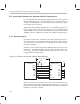
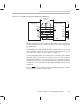
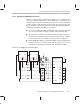
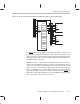
Table Of Contents
- Read This First
- Contents
- Figures
- Tables
- Examples
- Cautions
- Introduction
- Architectural Overview
- Central Processing Unit
- Memory and I/O Spaces
- Program Control
- Addressing Modes
- Assembly Language Instructions
- Instruction Set Summary
- How To Use the Instruction Descriptions
- Instruction Descriptions
- ABS
- ABS
- ADD
- ADD
- ADD
- ADD
- ADDC
- ADDC
- ADDS
- ADDS
- ADDT
- ADDT
- ADRK
- AND
- AND
- AND
- APAC
- APAC
- B
- BACC
- BANZ
- BANZ
- BCND
- BCND
- BIT
- BIT
- BITT
- BITT
- BLDD
- BLDD
- BLDD
- BLDD
- BLDD
- BLPD
- BLPD
- BLPD
- BLPD
- CALA
- CALL
- CC
- CC
- CLRC
- CLRC
- CMPL
- CMPR
- DMOV
- DMOV
- IDLE
- IN
- IN
- INTR
- LACC
- LACC
- LACC
- LACL
- LACL
- LACL
- LACT
- LACT
- LAR
- LAR
- LAR
- LDP
- LDP
- LPH
- LPH
- LST
- LST
- LST
- LST
- LT
- LT
- LTA
- LTA
- LTD
- LTD
- LTD
- LTP
- LTP
- LTS
- LTS
- MAC
- MAC
- MAC
- MAC
- MACD
- MACD
- MACD
- MACD
- MACD
- MAR
- MAR
- MPY
- MPY
- MPY
- MPYA
- MPYA
- MPYS
- MPYS
- MPYU
- MPYU
- NEG
- NEG
- NMI
- NOP
- NORM
- NORM
- NORM
- OR
- OR
- OR
- OUT
- OUT
- PAC
- POP
- POP
- POPD
- POPD
- PSHD
- PSHD
- PUSH
- RET
- RETC
- ROL
- ROR
- RPT
- RPT
- SACH
- SACH
- SACL
- SACL
- SAR
- SAR
- SBRK
- SETC
- SETC
- SFL
- SFR
- SFR
- SPAC
- SPH
- SPH
- SPL
- SPL
- SPLK
- SPLK
- SPM
- SQRA
- SQRA
- SQRS
- SQRS
- SST
- SST
- SUB
- SUB
- SUB
- SUB
- SUBB
- SUBB
- SUBC
- SUBC
- SUBS
- SUBS
- SUBT
- SUBT
- TBLR
- TBLR
- TBLR
- TBLW
- TBLW
- TBLW
- TRAP
- XOR
- XOR
- XOR
- ZALR
- ZALR
- On-Chip Peripherals
- Synchronous Serial Port
- Asynchronous Serial Port
- TMS320C209
- Register Summary
- TMS320C1x/C2x/C2xx/C5x Instruction Set Comparison
- Program Examples
- Submitting ROM Codes to TI
- Design Considerations for Using XDS510 Emulator
- E.1 Designing Your Target System’s Emulator Connector (14-Pin Header)
- E.2 Bus Protocol
- E.3 Emulator Cable Pod
- E.4 Emulator Cable Pod Signal Timing
- E.5 Emulation Timing Calculations
- E.6 Connections Between the Emulator and the Target System
- E.7 Physical Dimensions for the 14-Pin Emulator Connector
- E.8 Emulation Design Considerations
- Glossary
- Index

Connections Between the Emulator and the Target System
E-13
Design Considerations for Using XDS510 Emulator
E.6.3 Configuring Multiple Processors
Figure E–7 shows a typical daisy-chained multiprocessor configuration that
meets the minimum requirements of the IEEE 1149.1 specification. The
emulation signals are buffered to isolate the processors from the emulator and
provide adequate signal drive for the target system. One of the benefits of this
interface is that you can slow down the test clock to eliminate timing problems.
Follow these guidelines for multiprocessor support:
The processor TMS, TDI, TDO, and TCK signals must be buffered through
the same physical device package for better control of timing skew.
The input buffers for TMS, TDI, and TCK should have pullup resistors con-
nected to V
CC
to hold these signals at a known value when the emulator
is not connected. A resistor value of 4.7 kΩ or greater is suggested.
Buffering EMU0 and EMU1 is optional but highly recommended to provide
isolation. These are not critical signals and do not have to be buffered
through the same physical package as TMS, TCK, TDI, and TDO.
Figure E–7. Multiprocessor Connections
TDITDI TDOTDO
JTAG deviceJTAG device
V
CC
Emulator header
GND
12
10
8
6
4
5
GND
GND
GND
GND
GND
PD
TCK_RET
TCK
TDO
TDI
TMS
TRST
EMU1
EMU0
9
11
7
3
1
2
14
13
TMS
TCK
TRST
EMU0
EMU1
TMS
TCK
TRST
EMU0
EMU1
V
CC