
User manual
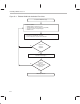
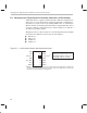

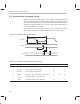
Table Of Contents
- Read This First
- Contents
- Figures
- Tables
- Examples
- Cautions
- Introduction
- Architectural Overview
- Central Processing Unit
- Memory and I/O Spaces
- Program Control
- Addressing Modes
- Assembly Language Instructions
- Instruction Set Summary
- How To Use the Instruction Descriptions
- Instruction Descriptions
- ABS
- ABS
- ADD
- ADD
- ADD
- ADD
- ADDC
- ADDC
- ADDS
- ADDS
- ADDT
- ADDT
- ADRK
- AND
- AND
- AND
- APAC
- APAC
- B
- BACC
- BANZ
- BANZ
- BCND
- BCND
- BIT
- BIT
- BITT
- BITT
- BLDD
- BLDD
- BLDD
- BLDD
- BLDD
- BLPD
- BLPD
- BLPD
- BLPD
- CALA
- CALL
- CC
- CC
- CLRC
- CLRC
- CMPL
- CMPR
- DMOV
- DMOV
- IDLE
- IN
- IN
- INTR
- LACC
- LACC
- LACC
- LACL
- LACL
- LACL
- LACT
- LACT
- LAR
- LAR
- LAR
- LDP
- LDP
- LPH
- LPH
- LST
- LST
- LST
- LST
- LT
- LT
- LTA
- LTA
- LTD
- LTD
- LTD
- LTP
- LTP
- LTS
- LTS
- MAC
- MAC
- MAC
- MAC
- MACD
- MACD
- MACD
- MACD
- MACD
- MAR
- MAR
- MPY
- MPY
- MPY
- MPYA
- MPYA
- MPYS
- MPYS
- MPYU
- MPYU
- NEG
- NEG
- NMI
- NOP
- NORM
- NORM
- NORM
- OR
- OR
- OR
- OUT
- OUT
- PAC
- POP
- POP
- POPD
- POPD
- PSHD
- PSHD
- PUSH
- RET
- RETC
- ROL
- ROR
- RPT
- RPT
- SACH
- SACH
- SACL
- SACL
- SAR
- SAR
- SBRK
- SETC
- SETC
- SFL
- SFR
- SFR
- SPAC
- SPH
- SPH
- SPL
- SPL
- SPLK
- SPLK
- SPM
- SQRA
- SQRA
- SQRS
- SQRS
- SST
- SST
- SUB
- SUB
- SUB
- SUB
- SUBB
- SUBB
- SUBC
- SUBC
- SUBS
- SUBS
- SUBT
- SUBT
- TBLR
- TBLR
- TBLR
- TBLW
- TBLW
- TBLW
- TRAP
- XOR
- XOR
- XOR
- ZALR
- ZALR
- On-Chip Peripherals
- Synchronous Serial Port
- Asynchronous Serial Port
- TMS320C209
- Register Summary
- TMS320C1x/C2x/C2xx/C5x Instruction Set Comparison
- Program Examples
- Submitting ROM Codes to TI
- Design Considerations for Using XDS510 Emulator
- E.1 Designing Your Target System’s Emulator Connector (14-Pin Header)
- E.2 Bus Protocol
- E.3 Emulator Cable Pod
- E.4 Emulator Cable Pod Signal Timing
- E.5 Emulation Timing Calculations
- E.6 Connections Between the Emulator and the Target System
- E.7 Physical Dimensions for the 14-Pin Emulator Connector
- E.8 Emulation Design Considerations
- Glossary
- Index
Emulator Cable Pod
E-5
Design Considerations for Using XDS510 Emulator
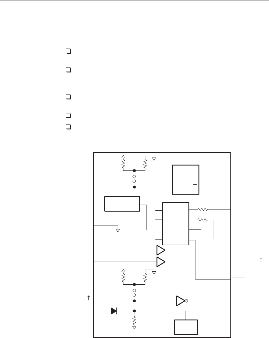
E.3 Emulator Cable Pod
Figure E–2 shows a portion of the emulator cable pod. The functional features
of the pod are:
TDO and TCK_RET can be parallel-terminated inside the pod if required
by the application. By default, these signals are not terminated.
TCK is driven with a 74LVT240 device. Because of the high-current drive
(32-mA I
OL
/I
OH
), this signal can be parallel-terminated. If TCK is tied to
TCK_RET, you can use the parallel terminator in the pod.
TMS and TDI can be generated from the falling edge of TCK_RET, accord-
ing to the IEEE 1149.1 bus slave device timing rules.
TMS and TDI are series-terminated to reduce signal reflections.
A 10.368-MHz test clock source is provided. You can also provide your
own test clock for greater flexibility.
Figure E–2. Emulator Cable Pod Interface
100 Ω
TL7705A
RESIN
270 Ω
JP2
180 Ω
TCK_RET (pin 9)
EMU1 (pin 14)
EMU0 (pin 13)
74AS1034
GND (pins 4,6,8,10,12)
TRST
(pin 2)
TCK (pin 11)
10.368 MHz
33 Ω
33 Ω
TDI (pin 3)
TMS (pin 1)
TDO (pin 7)
74LVT240
180 Ω
JP1
270 Ω
74F175
Q
Q
D
PD(V
CC
) (pin 5)
5 V
5 V
74AS1004
Y
Y
Y
Y
A
†
The emulator pod uses TCK_RET as its clock source for internal synchronization. TCK is provided as an
optional target system test clock source.