
User manual

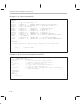
Table Of Contents
- Read This First
- Contents
- Figures
- Tables
- Examples
- Cautions
- Introduction
- Architectural Overview
- Central Processing Unit
- Memory and I/O Spaces
- Program Control
- Addressing Modes
- Assembly Language Instructions
- Instruction Set Summary
- How To Use the Instruction Descriptions
- Instruction Descriptions
- ABS
- ABS
- ADD
- ADD
- ADD
- ADD
- ADDC
- ADDC
- ADDS
- ADDS
- ADDT
- ADDT
- ADRK
- AND
- AND
- AND
- APAC
- APAC
- B
- BACC
- BANZ
- BANZ
- BCND
- BCND
- BIT
- BIT
- BITT
- BITT
- BLDD
- BLDD
- BLDD
- BLDD
- BLDD
- BLPD
- BLPD
- BLPD
- BLPD
- CALA
- CALL
- CC
- CC
- CLRC
- CLRC
- CMPL
- CMPR
- DMOV
- DMOV
- IDLE
- IN
- IN
- INTR
- LACC
- LACC
- LACC
- LACL
- LACL
- LACL
- LACT
- LACT
- LAR
- LAR
- LAR
- LDP
- LDP
- LPH
- LPH
- LST
- LST
- LST
- LST
- LT
- LT
- LTA
- LTA
- LTD
- LTD
- LTD
- LTP
- LTP
- LTS
- LTS
- MAC
- MAC
- MAC
- MAC
- MACD
- MACD
- MACD
- MACD
- MACD
- MAR
- MAR
- MPY
- MPY
- MPY
- MPYA
- MPYA
- MPYS
- MPYS
- MPYU
- MPYU
- NEG
- NEG
- NMI
- NOP
- NORM
- NORM
- NORM
- OR
- OR
- OR
- OUT
- OUT
- PAC
- POP
- POP
- POPD
- POPD
- PSHD
- PSHD
- PUSH
- RET
- RETC
- ROL
- ROR
- RPT
- RPT
- SACH
- SACH
- SACL
- SACL
- SAR
- SAR
- SBRK
- SETC
- SETC
- SFL
- SFR
- SFR
- SPAC
- SPH
- SPH
- SPL
- SPL
- SPLK
- SPLK
- SPM
- SQRA
- SQRA
- SQRS
- SQRS
- SST
- SST
- SUB
- SUB
- SUB
- SUB
- SUBB
- SUBB
- SUBC
- SUBC
- SUBS
- SUBS
- SUBT
- SUBT
- TBLR
- TBLR
- TBLR
- TBLW
- TBLW
- TBLW
- TRAP
- XOR
- XOR
- XOR
- ZALR
- ZALR
- On-Chip Peripherals
- Synchronous Serial Port
- Asynchronous Serial Port
- TMS320C209
- Register Summary
- TMS320C1x/C2x/C2xx/C5x Instruction Set Comparison
- Program Examples
- Submitting ROM Codes to TI
- Design Considerations for Using XDS510 Emulator
- E.1 Designing Your Target System’s Emulator Connector (14-Pin Header)
- E.2 Bus Protocol
- E.3 Emulator Cable Pod
- E.4 Emulator Cable Pod Signal Timing
- E.5 Emulation Timing Calculations
- E.6 Connections Between the Emulator and the Target System
- E.7 Physical Dimensions for the 14-Pin Emulator Connector
- E.8 Emulation Design Considerations
- Glossary
- Index

D-1
Appendix A
Submitting ROM Codes to TI
The size of a printed circuit board is a consideration in many DSP applications.
To make full use of the board space, Texas Instruments offers this ROM code
option that reduces the chip count and provides a single-chip solution. This op-
tion allows you to use a code-customized processor for a specific application
while taking advantage of:
Greater memory expansion
Lower system cost
Less hardware and wiring
Smaller PCB
If a routine or algorithm is used often, it can be programmed into the on-chip
ROM of a TMS320 DSP. TMS320 programs can also be expanded by using
external memory; this reduces chip count and allows for a more flexible pro-
gram memory. Multiple functions are easily implemented by a single device,
thus enhancing system capabilities.
TMS320 development tools are used to develop, test, refine, and finalize the
algorithms. The microprocessor/microcomputer (MP/MC
) mode is available
on all ROM-coded TMS320 DSP devices when accesses to either on-chip or
off-chip memory are required. The microprocessor mode is used to develop,
test, and refine a system application. In this mode of operation, the TMS320
acts as a standard microprocessor by using external program memory. When
the algorithm has been finalized, the code can be submitted to Texas Instru-
ments for masking into the on-chip program ROM. At that time, the TMS320
becomes a microcomputer that executes customized programs from the on-
chip ROM. Should the code need changing or upgrading, the TMS320 can
once again be used in the microprocessor mode. This shortens the field-
upgrade time and avoids the possibility of inventory obsolescence.
Figure D–1 illustrates the procedural flow for developing and ordering
TMS320 masked parts. When ordering, there is a one-time, nonrefundable
charge for mask tooling. A minimum production order per year is required for
any masked-ROM device. ROM codes will be deleted from the TI system one
year after the final delivery.
Appendix D