
User manual
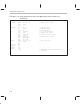

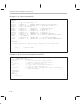
Table Of Contents
- Read This First
- Contents
- Figures
- Tables
- Examples
- Cautions
- Introduction
- Architectural Overview
- Central Processing Unit
- Memory and I/O Spaces
- Program Control
- Addressing Modes
- Assembly Language Instructions
- Instruction Set Summary
- How To Use the Instruction Descriptions
- Instruction Descriptions
- ABS
- ABS
- ADD
- ADD
- ADD
- ADD
- ADDC
- ADDC
- ADDS
- ADDS
- ADDT
- ADDT
- ADRK
- AND
- AND
- AND
- APAC
- APAC
- B
- BACC
- BANZ
- BANZ
- BCND
- BCND
- BIT
- BIT
- BITT
- BITT
- BLDD
- BLDD
- BLDD
- BLDD
- BLDD
- BLPD
- BLPD
- BLPD
- BLPD
- CALA
- CALL
- CC
- CC
- CLRC
- CLRC
- CMPL
- CMPR
- DMOV
- DMOV
- IDLE
- IN
- IN
- INTR
- LACC
- LACC
- LACC
- LACL
- LACL
- LACL
- LACT
- LACT
- LAR
- LAR
- LAR
- LDP
- LDP
- LPH
- LPH
- LST
- LST
- LST
- LST
- LT
- LT
- LTA
- LTA
- LTD
- LTD
- LTD
- LTP
- LTP
- LTS
- LTS
- MAC
- MAC
- MAC
- MAC
- MACD
- MACD
- MACD
- MACD
- MACD
- MAR
- MAR
- MPY
- MPY
- MPY
- MPYA
- MPYA
- MPYS
- MPYS
- MPYU
- MPYU
- NEG
- NEG
- NMI
- NOP
- NORM
- NORM
- NORM
- OR
- OR
- OR
- OUT
- OUT
- PAC
- POP
- POP
- POPD
- POPD
- PSHD
- PSHD
- PUSH
- RET
- RETC
- ROL
- ROR
- RPT
- RPT
- SACH
- SACH
- SACL
- SACL
- SAR
- SAR
- SBRK
- SETC
- SETC
- SFL
- SFR
- SFR
- SPAC
- SPH
- SPH
- SPL
- SPL
- SPLK
- SPLK
- SPM
- SQRA
- SQRA
- SQRS
- SQRS
- SST
- SST
- SUB
- SUB
- SUB
- SUB
- SUBB
- SUBB
- SUBC
- SUBC
- SUBS
- SUBS
- SUBT
- SUBT
- TBLR
- TBLR
- TBLR
- TBLW
- TBLW
- TBLW
- TRAP
- XOR
- XOR
- XOR
- ZALR
- ZALR
- On-Chip Peripherals
- Synchronous Serial Port
- Asynchronous Serial Port
- TMS320C209
- Register Summary
- TMS320C1x/C2x/C2xx/C5x Instruction Set Comparison
- Program Examples
- Submitting ROM Codes to TI
- Design Considerations for Using XDS510 Emulator
- E.1 Designing Your Target System’s Emulator Connector (14-Pin Header)
- E.2 Bus Protocol
- E.3 Emulator Cable Pod
- E.4 Emulator Cable Pod Signal Timing
- E.5 Emulation Timing Calculations
- E.6 Connections Between the Emulator and the Target System
- E.7 Physical Dimensions for the 14-Pin Emulator Connector
- E.8 Emulation Design Considerations
- Glossary
- Index

Introduction to Generating Boot Loader Code
C-24
Example C–15. Linker Command File
MEMORY
{
PAGE 0: /* PM – Program memory */
EX1_PM :ORIGIN=0H , LENGTH=0FEFFH /* External program RAM */
B0_PM :ORIGIN=0FF00H, LENGTH=0100H /* BLOCK MAP IN CNF=1 */
PAGE 1: /* DM – Data memory */
REGS :ORIGIN=0H , LENGTH=60H /* MEM–MAPPED REGS */
BLK_B2 :ORIGIN=60H , LENGTH=20H /* BLOCK B2 */
BLK_B0 :ORIGIN=200H , LENGTH=100H /* BLOCK B0, */
BLK_B1 :ORIGIN=300H , LENGTH=100H /* BLOCK B1 */
EX1_DM :ORIGIN=0800H , LENGTH=7800H /* EXTERNAL DATA RAM */
GM_DM :ORIGIN=8000H , LENGTH=8000H /* External DATA RAM AS GLOBAL */
PAGE 2: /* I/O SPACE */
IO_IN :ORIGIN=0FF00H, LENGTH=0FFH /* I/O MAPPED PERIPHERAL */
IO_EX :ORIGIN=0000H , LENGTH=0FF00H /* EXT. I/O MAPPED PERIPHERAL */
}
SECTIONS
/* Linker directive to specify section placement in the memory map */
{
.text :{} > EX1_PM PAGE 0
}
Example C–16. Hex Conversion Utility Command File
dsphex boot.cmd
/* boot.cmd file an example */
test.out /* File for boot code in COFF format*/
–i /* option to generate Intel hex format */
–o test.i0 /* Name of the output file */
–byte /* 16–bit code is converted into byte */
/* stack to suit 8–bit ROM. */
–order MS /* The byte order is higher byte first followed by */
/* lower order byte */
–memwidth 8
–romwidth 8
–boot
SECTIONS
{ .text:boot }