
User manual
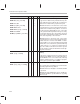
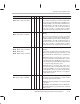
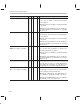
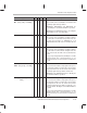
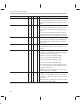
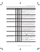
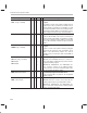
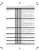
Table Of Contents
- Read This First
- Contents
- Figures
- Tables
- Examples
- Cautions
- Introduction
- Architectural Overview
- Central Processing Unit
- Memory and I/O Spaces
- Program Control
- Addressing Modes
- Assembly Language Instructions
- Instruction Set Summary
- How To Use the Instruction Descriptions
- Instruction Descriptions
- ABS
- ABS
- ADD
- ADD
- ADD
- ADD
- ADDC
- ADDC
- ADDS
- ADDS
- ADDT
- ADDT
- ADRK
- AND
- AND
- AND
- APAC
- APAC
- B
- BACC
- BANZ
- BANZ
- BCND
- BCND
- BIT
- BIT
- BITT
- BITT
- BLDD
- BLDD
- BLDD
- BLDD
- BLDD
- BLPD
- BLPD
- BLPD
- BLPD
- CALA
- CALL
- CC
- CC
- CLRC
- CLRC
- CMPL
- CMPR
- DMOV
- DMOV
- IDLE
- IN
- IN
- INTR
- LACC
- LACC
- LACC
- LACL
- LACL
- LACL
- LACT
- LACT
- LAR
- LAR
- LAR
- LDP
- LDP
- LPH
- LPH
- LST
- LST
- LST
- LST
- LT
- LT
- LTA
- LTA
- LTD
- LTD
- LTD
- LTP
- LTP
- LTS
- LTS
- MAC
- MAC
- MAC
- MAC
- MACD
- MACD
- MACD
- MACD
- MACD
- MAR
- MAR
- MPY
- MPY
- MPY
- MPYA
- MPYA
- MPYS
- MPYS
- MPYU
- MPYU
- NEG
- NEG
- NMI
- NOP
- NORM
- NORM
- NORM
- OR
- OR
- OR
- OUT
- OUT
- PAC
- POP
- POP
- POPD
- POPD
- PSHD
- PSHD
- PUSH
- RET
- RETC
- ROL
- ROR
- RPT
- RPT
- SACH
- SACH
- SACL
- SACL
- SAR
- SAR
- SBRK
- SETC
- SETC
- SFL
- SFR
- SFR
- SPAC
- SPH
- SPH
- SPL
- SPL
- SPLK
- SPLK
- SPM
- SQRA
- SQRA
- SQRS
- SQRS
- SST
- SST
- SUB
- SUB
- SUB
- SUB
- SUBB
- SUBB
- SUBC
- SUBC
- SUBS
- SUBS
- SUBT
- SUBT
- TBLR
- TBLR
- TBLR
- TBLW
- TBLW
- TBLW
- TRAP
- XOR
- XOR
- XOR
- ZALR
- ZALR
- On-Chip Peripherals
- Synchronous Serial Port
- Asynchronous Serial Port
- TMS320C209
- Register Summary
- TMS320C1x/C2x/C2xx/C5x Instruction Set Comparison
- Program Examples
- Submitting ROM Codes to TI
- Design Considerations for Using XDS510 Emulator
- E.1 Designing Your Target System’s Emulator Connector (14-Pin Header)
- E.2 Bus Protocol
- E.3 Emulator Cable Pod
- E.4 Emulator Cable Pod Signal Timing
- E.5 Emulation Timing Calculations
- E.6 Connections Between the Emulator and the Target System
- E.7 Physical Dimensions for the 14-Pin Emulator Connector
- E.8 Emulation Design Considerations
- Glossary
- Index
Instruction Set Comparison Table
B-21
TMS320C1x/C2x/C2xx/C5x Instruction Set Comparison
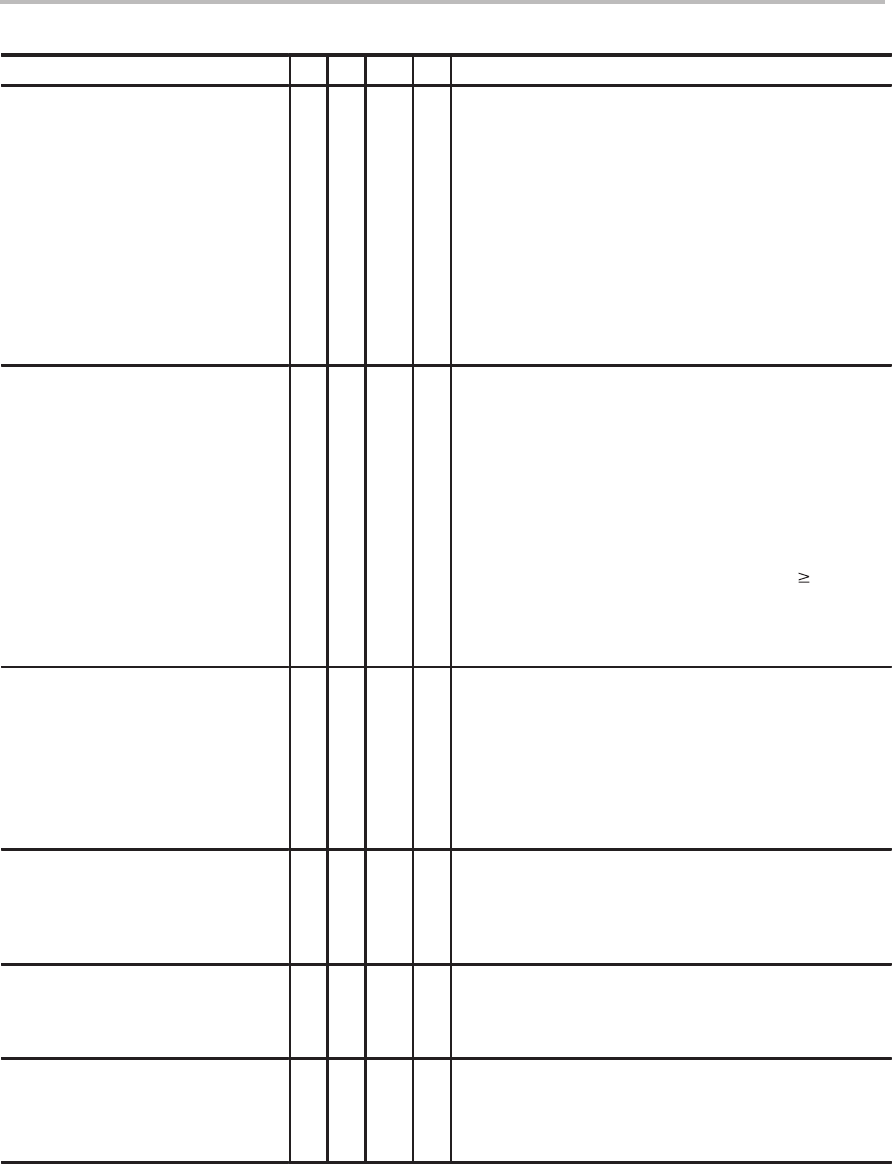
Syntax
Description5x2xx2x1x
LDP
dma
LDP {
ind
} [
, next ARP
]
LDP #
k
√
√
√
√
√
√
√
√
√
√
Load Data-Memory Page Pointer
TMS320C1x devices: Load the LSB of the contents of
the addressed data-memory location into the DP regis-
ter. All high-order bits are ignored. DP = 0 defines page
0 (words 0–127), and DP = 1 defines page 1 (words
128–143/255).
TMS320C2x, TMS320C2xx, and TMS320C5x de-
vices: Load the 9 LSBs of the addressed data-memory
location or a 9-bit immediate value into the DP register.
The DP and 7-bit data-memory address are concate-
nated to form 16-bit data-memory addresses.
LDPK
1-bit constant
LDPK
9-bit constant
√
√ √ √
Load Data-Memory Page Pointer Immediate
TMS320C1x devices: Load a 1-bit immediate value
into the DP register. DP = 0 defines page 0 (words
0–127), and DP = 1 defines page 1 (words
128–143/255).
TMS320C2x, TMS320C2xx, and TMS320C5x de-
vices: Load a 9-bit immediate into the DP register. The
DP and 7-bit data-memory address are concatenated
to form 16-bit data-memory addresses. DP 8 speci-
fies external data memory. DP = 4 through 7 specifies
on-chip RAM blocks B0 or B1. Block B2 is located in
the upper 32 words of page 0.
LMMR
dma,
#
lk
LMMR {
ind
}
,
#
lk
[
, next ARP
]
√
√
Load Memory-Mapped Register
Load the contents of the memory-mapped register
pointed at by the 7 LSBs of the direct or indirect data-
memory value into the long immediate addressed
data-memory location. The 9 MSBs of the data-
memory address are cleared, regardless of the current
value of DP or the 9 MSBs of AR (ARP).
LPH
dma
LPH {
ind
} [
, next ARP
]
√
√
√
√
√
√
Load High P Register
Load the contents of the addressed data-memory lo-
cation into the 16 MSBs of the P register; the LSBs are
not affected.
LRLK
AR, lk
√ √ √
Load Auxiliary Register Long Immediate
Load a 16-bit immediate value into the designated aux-
iliary register.
LST
dma
LST {
ind
} [
, next ARP
]
√
√
√
√
√
√
√
√
Load Status Register
Load the contents of the addressed data-memory
location into the ST (TMS320C1x) or into ST0
(TMS320C2x/2xx/5x).